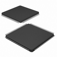
CY7C056V-12AXC Cypress Semiconductor Corp, CY7C056V-12AXC Datasheet - Page 8

CY7C056V-12AXC
Manufacturer Part Number
CY7C056V-12AXC
Description
IC SRAM 576KBIT 12NS 144LQFP
Manufacturer
Cypress Semiconductor Corp
Specifications of CY7C056V-12AXC
Format - Memory
RAM
Memory Type
SRAM - Dual Port, Asynchronous
Memory Size
576K (16K x 36)
Speed
12ns
Interface
Parallel
Voltage - Supply
3 V ~ 3.6 V
Operating Temperature
0°C ~ 70°C
Package / Case
144-LQFP
Density
576Kb
Access Time (max)
12ns
Sync/async
Asynchronous
Architecture
Not Required
Clock Freq (max)
Not RequiredMHz
Operating Supply Voltage (typ)
3.3V
Address Bus
14b
Package Type
TQFP
Operating Temp Range
0C to 70C
Number Of Ports
2
Supply Current
385mA
Operating Supply Voltage (min)
3.135V
Operating Supply Voltage (max)
3.465V
Operating Temperature Classification
Commercial
Mounting
Surface Mount
Pin Count
144
Word Size
36b
Number Of Words
16K
Lead Free Status / RoHS Status
Lead free / RoHS Compliant
Available stocks
Company
Part Number
Manufacturer
Quantity
Price
Company:
Part Number:
CY7C056V-12AXC
Manufacturer:
CY
Quantity:
8
Company:
Part Number:
CY7C056V-12AXC
Manufacturer:
ON
Quantity:
6 393
Company:
Part Number:
CY7C056V-12AXC
Manufacturer:
Cypress Semiconductor Corp
Quantity:
10 000
Electrical Characteristics
Capacitance
Notes
Document #: 38-06055 Rev. *E
V
V
V
V
I
I
I
I
I
I
8. Deselection for a port occurs if CE
9. f
10. Tested initially and after any design or process changes that may affect these parameters.
C
C
OZ
CC
SB1
SB2
SB3
SB4
Parameter
OH
OL
IH
IL
IN
OUT
MAX
= 1/t
Parameter
RC
= All inputs cycling at f = 1/t
Output HIGH voltage
(V
Output LOW voltage
(V
Input HIGH voltage
Input LOW voltage
Output leakage current
Operating current (V
I
Standby current (Both ports TTL level
and deselected)
f = f
Standby current (One port TTL
level and deselected)
f = f
Standby current (Both ports CMOS
level and deselected) f =0
Standby current (One Port CMOS
level and deselected) f = f
OUT
DD
DD
[10]
MAX
MAX
= 0 mA) output disabled
= Min., I
= Min., I
OH
OL
Input capacitance
Output capacitance
0
= +4.0 mA)
= –4.0 mA)
is HIGH or if CE
RC
DD
Description
(except Output Enable). f = 0 means no address or control lines change. This applies only to inputs at CMOS level standby I
Over the Operating Range
Description
= Max.,
MAX
1
[9]
is LOW.
Commercial
Commercial
Commercial
Commercial
Commercial
Industrial
Industrial
Industrial
Industrial
Industrial
T
V
A
DD
= 25
[8]
= 3.3 V
Test Conditions
C, f = 1 MHz,
Min
–10
2.4
2.0
–
–
–
0.01
-12
Typ
250
180
160
55
–
–
–
–
–
Max
385
240
210
0.4
0.8
CY7C056V
CY7C057V
10
75
–
–
1
Min
–10
2.4
2.0
–
–
–
Max
10
10
0.01
0.01
Typ
240
265
175
190
155
170
-15
50
65
–
CY7C056V
CY7C057V
Max
360
385
230
255
200
215
0.4
0.8
10
70
95
–
–
1
1
Page 8 of 26
Unit
pF
pF
Unit
mA
mA
mA
mA
mA
mA
mA
mA
mA
mA
A
V
V
V
V
SB3
[+] Feedback
.


