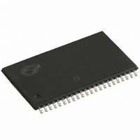
CY7C1021BNL-15ZXCT Cypress Semiconductor Corp, CY7C1021BNL-15ZXCT Datasheet

CY7C1021BNL-15ZXCT
Specifications of CY7C1021BNL-15ZXCT
Related parts for CY7C1021BNL-15ZXCT
CY7C1021BNL-15ZXCT Summary of contents
Page 1
... COLUMN DECODER Note: 1. For best-practice recommendations, please refer to the Cypress application note “System Design Guidelines” on http://www.cypress.com Cypress Semiconductor Corporation Document #: 001-06494 Rev. *A 1-Mbit (64K x 16) Static RAM Writing to the device is accomplished by taking Chip Enable (CE) and Write Enable (WE) inputs LOW. If Byte Low Enable ...
Page 2
Selection Guide Maximum Access Time (ns) Maximum Operating Current (mA) Maximum CMOS Standby Current (mA) Com’l / Ind’l Pin Definitions Pin Name SOJ, TSOP–Pin Number A –A 1–5,18–21, 24–27, 42– I/O –I/O 7–10, 13–16, 29–32 35–38 ...
Page 3
Maximum Ratings (Above which the useful life may be impaired. For user guide- lines, not tested.) Storage Temperature ................................. –65°C to +150°C Ambient Temperature with Power Applied............................................. –55°C to +125°C Supply Voltage on V Relative to GND CC DC Voltage ...
Page 4
Thermal Resistance Parameter Description Θ Thermal Resistance Test conditions follow standard test methods JA (Junction to Ambient) and procedures for measuring thermal Θ impedance, per EIA / JESD51. Thermal Resistance JC (Junction to Case) AC Test Loads and Waveforms ...
Page 5
... Notes: 8. The internal write time of the memory is defined by the overlap of CE LOW, WE LOW and BHE / BLE LOW. CE, WE and BHE / BLE must be LOW to initiate a write, and the transition of these signals can terminate the write. The input data set-up and hold timing should be referenced to the leading edge of the signal that terminates the write ...
Page 6
Switching Waveforms (continued) [12, 13] Write Cycle No. 1 (CE Controlled) ADDRESS ADDRESS BHE, BLE DATA I/O Write Cycle No. 2 (BLE or BHE Controlled) ADDRESS t SA BHE, BLE WE CE DATA I/O Notes: 11. ...
Page 7
Switching Waveforms (continued) Write Cycle No. 3 (WE Controlled, OE LOW) ADDRESS BHE, BLE DATA I/O Truth Table BLE BHE I High ...
Page 8
... CY7C1021BN-12VC CY7C1021BN-12VXC CY7C1021BN-12ZC CY7C1021BN-12ZXC CY7C1021BN-12VI CY7C1021BN-12VXI 15 CY7C1021BN-15VC CY7C1021BN-15VXC CY7C1021BNL-15VXC CY7C1021BN-15ZC CY7C1021BN-15ZXC CY7C1021BNL-15ZC CY7C1021BNL-15ZXC CY7C1021BN-15VI CY7C1021BN-15VXI CY7C1021BN-15ZI CY7C1021BNL-15ZI CY7C1021BN-15ZXI CY7C1021BNL-15ZXI CY7C1021BNL-15ZSXA CY7C1021BN-15VXE CY7C1021BN-15ZSXE Package Diagrams 44 1 1.120 1.130 0.095 0.115 0.023 0.045 0.033 MAX. 0.013 0.023 Document #: 001-06494 Rev. *A Package Diagram Package Type ...
Page 9
... Document #: 001-06494 Rev. *A © Cypress Semiconductor Corporation, 2006. The information contained herein is subject to change without notice. Cypress Semiconductor Corporation assumes no responsibility for the use of any circuitry other than circuitry embodied in a Cypress product. Nor does it convey or imply any license under patent or other rights. Cypress products are not warranted nor intended to be used for medical, life support, life saving, critical control or safety applications, unless pursuant to an express written agreement with Cypress ...
Page 10
Document History Page Document Title: CY7C1021BN/CY7C10211BN (64K x 16) Static RAM Document Number: 001-06494 Orig. of REV. ECN NO. Issue Date Change ** 423877 See ECN *A 505726 See ECN Document #: 001-06494 Rev. *A Description of Change NXR New ...


