CY7C199CNL-15VXC Cypress Semiconductor Corp, CY7C199CNL-15VXC Datasheet
CY7C199CNL-15VXC
Specifications of CY7C199CNL-15VXC


Related parts for CY7C199CNL-15VXC


CY7C199CNL-15VXC Summary of contents
Page 1
... Maximum Operating Current Maximum CMOS Standby Current (low power) Note 1. For best practices recommendations, refer to the Cypress application note System Design Guidelines on www.cypress.com. Cypress Semiconductor Corporation Document #: 001-06435 Rev. *B 256K (32K x 8) Static RAM General Description The CY7C199CN is a high performance CMOS Asynchronous SRAM organized as 32K by 8 bits that supports an asynchronous memory interface ...
Page 2
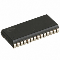
Pin Layout and Specifications 28 DIP ...
Page 3
Pin Description Pin Type Description A Input Address Inputs X CE Control Chip Enable IO Input or Output Data Input Outputs X OE Control Output Enable V Supply Power (5.0V Supply Ground SS WE Control Write Enable Truth ...
Page 4
DC Electrical Characteristics Over the Operating Range (–12, –15) Parameter Description V Input HIGH Voltage IH V Input LOW Voltage IL V Output HIGH Voltage Output LOW Voltage Operating Supply ...
Page 5
Capacitance [3] Parameter Description C Input Capacitance IN C Output Capacitance OUT Thermal Resistance [3] Parameter Description Θ Thermal Resistance JA (junction to ambient) Θ Thermal Resistance JC (junction to case) AC Test Loads ...
Page 6
... HZWE 7. The internal memory write time is defined by the overlap of CE LOW and WE LOW. CE and WE must be LOW to initiate a write, and the transition of any of these signals can terminate the write. The input data setup and hold timing must be referenced to the leading edge of the signal that terminates the write. ...
Page 7
Timing Waveforms Data Retention Waveform CDR CE [9, 10] Read Cycle 1 Address Data Out Previous Data Valid [11, 12] Read Cycle 2 Address CE OE High Z Data Out Current ...
Page 8
Timing Waveforms (continued) [13, 14, 15] Write Cycle 1 (WE controlled) Address HZOE Undefined Data In/Out see footnotes [14, 16, 17] Write Cycle 2 (CE controlled) Address CE WE High Z Data In/Out Notes ...
Page 9
Timing Waveforms (continued) Write Cycle 3 (WE controlled, OE low) Address Data Undefined In Out see footnotes Note 18. The cycle is WE controlled, OE LOW. The minimum write cycle time is the sum of t ...
Page 10
... CY7C199CN–15VXC 51-85031 CY7C199CN–15ZC 51-85071 CY7C199CN–15ZXC 51-85071 CY7C199CN–15VI 51-85031 CY7C199CNL–15VC 51-85031 CY7C199CNL–15VXC 51-85031 CY7C199CNL–15ZXC 51-85071 CY7C199CNL–15VXI 51-85031 20 CY7C199CN–20VC 51-85031 CY7C199CN–20ZI 51-85071 CY7C199CN–20ZXI 51-85071 25 CY7C199CN–25PC 51-85014 CY7C199CN–25PXC 51-85014 Document #: 001-06435 Rev. *B ...
Page 11
Package Diagrams Document #: 001-06435 Rev. *B Figure 1. 28-pin TSOP 13.4 mm), 51-85071 CY7C199CN 51-85071-*G Page ...
Page 12
Package Diagrams (continued) NOTE : 1. JEDEC STD REF MO088 2. BODY LENGTH DIMENSION DOES NOT INCLUDE MOLD PROTRUSION/END FLASH MOLD PROTRUSION/END FLASH SHALL NOT EXCEED 0.006 in (0.152 mm) PER SIDE MIN. 3. DIMENSIONS IN INCHES MAX ...
Page 13
... Document #: 001-06435 Rev. *B © Cypress Semiconductor Corporation, 2006-2007. The information contained herein is subject to change without notice. Cypress Semiconductor Corporation assumes no responsibility for the use of any circuitry other than circuitry embodied in a Cypress product. Nor does it convey or imply any license under patent or other rights. Cypress products are not warranted nor intended to be used for medical, life support, life saving, critical control or safety applications, unless pursuant to an express written agreement with Cypress ...
Page 14
Document History Page Document Title: CY7C199CN, 256K (32K x 8) Static RAM Document Number: 001-06435 Issue REV. ECN No. Date ** 430363 See ECN *A 684342 See ECN *B 839904 See ECN Document #: 001-06435 Rev. *B Orig. of Description ...