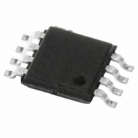
M93C46-RDS6TG STMicroelectronics, M93C46-RDS6TG Datasheet - Page 11

M93C46-RDS6TG
Manufacturer Part Number
M93C46-RDS6TG
Description
IC EEPROM 1KBIT 1MHZ 8TSSOP
Manufacturer
STMicroelectronics
Datasheet
1.M93C46-RDS6G.pdf
(30 pages)
Specifications of M93C46-RDS6TG
Format - Memory
EEPROMs - Serial
Memory Type
EEPROM
Memory Size
1K (128 x 8 or 64 x 16)
Speed
1MHz
Interface
Microwire, 3-Wire Serial
Voltage - Supply
1.8 V ~ 5.5 V
Operating Temperature
-40°C ~ 85°C
Package / Case
8-TSSOP
Lead Free Status / RoHS Status
Lead free / RoHS Compliant
Available stocks
Company
Part Number
Manufacturer
Quantity
Price
Figure 8. Write Sequence with One Clock Glitch
CLOCK PULSE COUNTER
In a noisy environment, the number of pulses re-
ceived on Serial Clock (C) may be greater than the
number delivered by the master (the microcontrol-
ler). This can lead to a misalignment of the instruc-
tion of one or more bits (as shown in Figure 8) and
may lead to the writing of erroneous data at an er-
roneous address.
To combat this problem, the M93Cx6 has an on-
chip counter that counts the clock pulses from the
start bit until the falling edge of the Chip Select In-
put (S). If the number of clock pulses received is
not the number expected, the WRITE, ERASE,
S
D
C
START
"0"
WRITE
"1"
M93C86, M93C76, M93C66, M93C56, M93C46, M93C06
An
Glitch
An-1
ERAL or WRAL instruction is aborted, and the
contents of the memory are not modified.
The number of clock cycles expected for each in-
struction, and for each member of the M93Cx6
family, are summarized in Table 4 to Table 6. For
example, a Write Data to Memory (WRITE) in-
struction on the M93C56 (or M93C66) expects 20
clock cycles (for the x8 organization) from the start
bit to the falling edge of Chip Select Input (S). That
is:
ARE SHIFTED BY ONE BIT
ADDRESS AND DATA
1 Start bit
+ 2 Op-code bits
+ 9 Address bits
+ 8 Data bits
An-2
D0
AI01395
11/30


