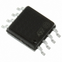
M95256-WMW6TG STMicroelectronics, M95256-WMW6TG Datasheet - Page 12

M95256-WMW6TG
Manufacturer Part Number
M95256-WMW6TG
Description
IC EEPROM 256KBIT 5MHZ 8SOIC
Manufacturer
STMicroelectronics
Datasheet
1.M95256-WMN6TP.pdf
(47 pages)
Specifications of M95256-WMW6TG
Format - Memory
EEPROMs - Serial
Memory Type
EEPROM
Memory Size
256K (32K x 8)
Speed
5MHz
Interface
SPI, 3-Wire Serial
Voltage - Supply
2.5 V ~ 5.5 V
Operating Temperature
-40°C ~ 85°C
Package / Case
8-SOIC (5.3mm Width), 8-SOP, 8-SOEIAJ
Lead Free Status / RoHS Status
Lead free / RoHS Compliant
Other names
497-8692-2
M95256-WMW6TG
M95256-WMW6TG
Available stocks
Company
Part Number
Manufacturer
Quantity
Price
Company:
Part Number:
M95256-WMW6TG
Manufacturer:
ST
Quantity:
4 300
Part Number:
M95256-WMW6TG
Manufacturer:
ST
Quantity:
20 000
Operating features
4.2
4.3
12/47
Figure 5.
Status Register
Figure 4
Status Register contains a number of status and control bits that can be read or set (as
appropriate) by specific instructions. For a detailed description of the Status Register bits,
see
Data protection and protocol control
Non-volatile memory devices can be used in environments that are particularly noisy, and
within applications that could experience problems if memory bytes are corrupted.
Consequently, the device features the following data protection mechanisms:
●
●
●
●
For any instruction to be accepted, and executed, Chip Select (S) must be driven high after
the rising edge of Serial Clock (C) for the last bit of the instruction, and before the next rising
edge of Serial Clock (C).
HOLD
Section 5.3: Read Status Register
C
Write and Write Status Register instructions are checked that they consist of a number
of clock pulses that is a multiple of eight, before they are accepted for execution.
All instructions that modify data must be preceded by a Write Enable (WREN)
instruction to set the Write Enable Latch (WEL) bit. This bit is returned to its reset state
by the following events:
–
–
–
–
The Block Protect (BP1, BP0) bits in the Status Register allow part of the memory to be
configured as read-only.
The Write Protect (W) signal is used to protect the Block Protect (BP1, BP0) bits of the
Status Register.
shows the position of the Status Register in the control logic of the device. The
Power-up
Write Disable (WRDI) instruction completion
Write Status Register (WRSR) instruction completion
Write (WRITE) instruction completion
Hold condition activation
Doc ID 12276 Rev 13
Condition
Hold
(RDSR).
M95256-DR, M95256, M95256-W, M95256-R
Condition
Hold
AI02029D


