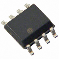
EPCS1SI8 Altera, EPCS1SI8 Datasheet - Page 19

EPCS1SI8
Manufacturer Part Number
EPCS1SI8
Description
IC CONFIG DEVICE 1MBIT 8-SOIC
Manufacturer
Altera
Series
EPCSr
Datasheet
1.EPCS1SI8.pdf
(38 pages)
Specifications of EPCS1SI8
Programmable Type
In System Programmable
Memory Size
1Mb
Voltage - Supply
3 V ~ 3.6 V
Operating Temperature
-40°C ~ 85°C
Package / Case
8-SOIC (0.154", 3.90mm Width)
Lead Free Status / RoHS Status
Contains lead / RoHS non-compliant
Other names
544-1241-5
Available stocks
Company
Part Number
Manufacturer
Quantity
Price
Company:
Part Number:
EPCS1SI8
Manufacturer:
ALTERA
Quantity:
22
Part Number:
EPCS1SI8
Manufacturer:
ALTERA/阿尔特拉
Quantity:
20 000
Company:
Part Number:
EPCS1SI8N
Manufacturer:
ALTERA
Quantity:
672
Chapter 3: Serial Configuration Devices (EPCS1, EPCS4, EPCS16, EPCS64, and EPCS128) Data Sheet
Serial Configuration Device Memory Access
Figure 3–9. Read Status Operation Timing Diagram
Figure 3–10. Write Status Operation Timing Diagram
© December 2009
DCLK
DATA
ASDI
nCS
Altera Corporation
Write Status Operation
The write status operation code is b'0000 0001, with the MSB listed first. Use the
write status operation to set the status register block protection bits. The write status
operation has no effect on the other bits. Therefore, you can implement this operation
to protect certain memory sectors, as defined in
setting the block protect bits, the protected memory sectors are treated as read-only
memory. You must execute the write enable operation before the write status
operation so the device sets the status register’s write enable latch bit to 1.
The write status operation is implemented by driving nCS low, followed by shifting in
the write status operation code and one data byte for the status register on the ASDI
pin.
driven high after the eighth bit of the data byte has been latched in, otherwise, the
write status operation is not executed.
Immediately after nCS drives high, the device initiates the self-timed write status
cycle. The self-timed write status cycle usually takes 5 ms for all serial configuration
devices and is guaranteed to be less than 15 ms (refer to t
account for this delay to ensure that the status register is written with desired block
protect bits. Alternatively, you can check the write in progress bit in the status register
by executing the read status operation while the self-timed write status cycle is in
progress. The write in progress bit is 1 during the self-timed write status cycle, and 0
when it is complete.
DCLK
DATA
ASDI
nCS
0
Figure 3–10
High Impedance
1
2
Operation Code
3
0
4
High Impedance
1
shows the timing diagram for the write status operation. nCS must be
5
2
6
Operation Code
3
7
MSB
4
7
8
5
6
9
6
Status Register Out
5
10
7
4
11
MSB
7
8
3
12
6
9
2
13
5
10
1
14
Status Register
4
11
0
15
MSB
3
12
7
Configuration Handbook (Complete Two-Volume Set)
Table 3–9
2
13
6
1
14
5
Status Register Out
0
15
4
WS
through
3
in
2
Table
1
Table
0
3–16). You must
7
3–13. After
3–19


