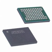
EPC16UC88N Altera, EPC16UC88N Datasheet - Page 16

EPC16UC88N
Manufacturer Part Number
EPC16UC88N
Description
IC CONFIG DEVICE 16MBIT 88-UBGA
Manufacturer
Altera
Series
EPCr
Specifications of EPC16UC88N
Programmable Type
In System Programmable
Memory Size
16Mb
Voltage - Supply
3 V ~ 3.6 V
Operating Temperature
0°C ~ 70°C
Package / Case
88-UBGA
Function
Configuration Device
Operating Supply Voltage (typ)
3.3V
Operating Supply Voltage (max)
3.6V
Operating Supply Voltage (min)
3V
Operating Temperature Classification
Commercial
Operating Temperature (min)
0C
Operating Temperature (max)
70C
Mounting
Surface Mount
Pin Count
88
Package Type
uBGA
Memory Type
Flash
Clock Frequency
66.7MHz
Supply Voltage Range
3V To 3.6V
Memory Case Style
BGA
No. Of Pins
88
Operating Temperature Range
0°C To +70°C
Access Time
90ns
Rohs Compliant
Yes
Lead Free Status / RoHS Status
Lead free / RoHS Compliant
Other names
544-1374
EPC16UC88N
EPC16UC88N
Available stocks
Company
Part Number
Manufacturer
Quantity
Price
Company:
Part Number:
EPC16UC88N
Manufacturer:
ALTERA
Quantity:
35
Company:
Part Number:
EPC16UC88N
Manufacturer:
ALTERA31EOL
Quantity:
184
Part Number:
EPC16UC88N
Manufacturer:
ALTERA/阿尔特拉
Quantity:
20 000
1–16
Configuration Handbook (Complete Two-Volume Set)
1
1
2. Using V
3. Using a high CE# disables the chip. The requirement for a write is a low CE# and
4. Using a high WE# prevent writes because a write only occurs when the WE# is low.
Performing all four methods simultaneously is the safest protection for the flash
content.
The ideal power-up sequence is as follows:
1. Power-up V
2. Maintain V
3. Power-up V
4. Drive RP# low during the entire power-up process. RP# must be released high
CE# and WE# must be high for the entire power-up sequence.
The ideal power-down sequence is as follows:
1. Drive RP# low for 100ns before power-down.
2. Power-down V
3. Power-down V
4. Drive RP# low during the entire power-down process.
CE# and WE# must be high for the entire power-down sequence.
The RP# pin is not internally connected to the controller. Therefore, an external
loop-back connection between C-RP# and F-RP# must be made on the board even
when you are not using the external device to the RP# pin with the loop-back. Always
tri-state RP# when the flash is not in use.
If an external power-up monitoring circuit is connected to the RP# pin with the
loop-back, use the following guidelines to avoid contention on the RP# line:
■
■
If the preceding guidelines cannot be completed within 50 ms, then the OE pin must
be driven low externally until RP# is ready to be released.
V
supply voltage input pin on the Intel flash. V
EPC devices.
low WE#. A high CE# by itself prevents writes from occurring.
within 25 ms after V
The power-up sequence on the 3.3-V supply should complete within 50 ms of
power-up. The 3.3-V V
should then be released.
RP# should be driven low by the power-up monitoring circuit during power-up.
After power-up, RP# should be tri-stated externally by the power-up monitoring
circuit.
PP
< V
PPLK
PP
< V
PP
means programming or writes cannot occur. V
CC
PP
< V
PPLK
.
.
PP
CC
PPLK
.
< V
, where the maximum value of V
PP
PPLK
until V
Chapter 1: Enhanced Configuration Devices (EPC4, EPC8, and EPC16) Data Sheet
is powered up.
CC
.
should reach the minimum V
CC
is fully powered up.
PP
is equivalent to the VCCW pin on
PPLK
© December 2009 Altera Corporation
CC
is 1 V, disables writes.
before 50 ms and RP#
PP
is a programming
Functional Description


