EPC16UC88N Altera, EPC16UC88N Datasheet - Page 28
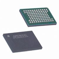
EPC16UC88N
Manufacturer Part Number
EPC16UC88N
Description
IC CONFIG DEVICE 16MBIT 88-UBGA
Manufacturer
Altera
Series
EPCr
Specifications of EPC16UC88N
Programmable Type
In System Programmable
Memory Size
16Mb
Voltage - Supply
3 V ~ 3.6 V
Operating Temperature
0°C ~ 70°C
Package / Case
88-UBGA
Function
Configuration Device
Operating Supply Voltage (typ)
3.3V
Operating Supply Voltage (max)
3.6V
Operating Supply Voltage (min)
3V
Operating Temperature Classification
Commercial
Operating Temperature (min)
0C
Operating Temperature (max)
70C
Mounting
Surface Mount
Pin Count
88
Package Type
uBGA
Memory Type
Flash
Clock Frequency
66.7MHz
Supply Voltage Range
3V To 3.6V
Memory Case Style
BGA
No. Of Pins
88
Operating Temperature Range
0°C To +70°C
Access Time
90ns
Rohs Compliant
Yes
Lead Free Status / RoHS Status
Lead free / RoHS Compliant
Other names
544-1374
EPC16UC88N
EPC16UC88N
Available stocks
Company
Part Number
Manufacturer
Quantity
Price
Company:

Part Number:
EPC16UC88N
Manufacturer:
ALTERA
Quantity:
35
Company:
Part Number:
EPC16UC88N
Manufacturer:
ALTERA31EOL
Quantity:
184
Part Number:
EPC16UC88N
Manufacturer:
ALTERA/阿尔特拉
Quantity:
20 000


1–28
IEEE Std. 1149.1 (JTAG) Boundary-Scan
Figure 1–6. JTAG Timing Waveforms
Table 1–13. JTAG Timing Parameters and Values
Configuration Handbook (Complete Two-Volume Set)
t
t
t
t
t
t
t
t
t
t
t
t
t
JCP
JCH
JCL
JPSU
JPH
JPCO
JPZX
JPXZ
JSSU
JSH
JSCO
JSZX
JSXZ
Symbol
Captured
TCK clock period
TCK clock high time
TCK clock low time
JTAG port setup time
JTAG port hold time
JTAG port clock output
JTAG port high impedance to valid output
JTAG port valid output to high impedance
Capture register setup time
Capture register hold time
Update register clock to output
Update register high-impedance to valid output
Update register valid output to high impedance
The enhanced configuration device provides JTAG BST circuitry that complies with
the IEEE Std. 1149.1-1990 specification. JTAG boundary-scan testing can be performed
before or after configuration, but not during configuration.
Figure 1–6
Driven
Table 1–13
device.
Signal
Signal
to be
to be
TMS
TDO
TCK
TDI
shows the timing requirements for the JTAG signals.
lists the timing parameters and values for the enhanced configuration
t
JCH
t
t
JSZX
JPZX
t
JCP
t
JSSU
Parameter
t
JCL
t
Chapter 1: Enhanced Configuration Devices (EPC4, EPC8, and EPC16) Data Sheet
JSH
t
t
JPCO
JSCO
t
JPSU
t
t
JPH
JSXZ
Min
100
50
50
20
45
—
—
—
20
45
—
—
—
t
JPXZ
IEEE Std. 1149.1 (JTAG) Boundary-Scan
© December 2009 Altera Corporation
Max
—
—
—
—
—
25
25
25
—
—
25
25
25
Unit
ns
ns
ns
ns
ns
ns
ns
ns
ns
ns
ns
ns
ns
Related parts for EPC16UC88N
Image
Part Number
Description
Manufacturer
Datasheet
Request
R

Part Number:
Description:
Configuration EPROMs For Flex Devices
Manufacturer:
Altera Corporation
Datasheet:

Part Number:
Description:
CYCLONE II STARTER KIT EP2C20N
Manufacturer:
Altera
Datasheet:

Part Number:
Description:
CPLD, EP610 Family, ECMOS Process, 300 Gates, 16 Macro Cells, 16 Reg., 16 User I/Os, 5V Supply, 35 Speed Grade, 24DIP
Manufacturer:
Altera Corporation
Datasheet:
Part Number:
Description:
CPLD, EP610 Family, ECMOS Process, 300 Gates, 16 Macro Cells, 16 Reg., 16 User I/Os, 5V Supply, 15 Speed Grade, 24DIP
Manufacturer:
Altera Corporation
Datasheet:
Part Number:
Description:
Manufacturer:
Altera Corporation
Datasheet:
Part Number:
Description:
CPLD, EP610 Family, ECMOS Process, 300 Gates, 16 Macro Cells, 16 Reg., 16 User I/Os, 5V Supply, 30 Speed Grade, 24DIP
Manufacturer:
Altera Corporation
Datasheet:
Part Number:
Description:
High-performance, low-power erasable programmable logic devices with 8 macrocells, 10ns
Manufacturer:
Altera Corporation
Datasheet:
Part Number:
Description:
High-performance, low-power erasable programmable logic devices with 8 macrocells, 7ns
Manufacturer:
Altera Corporation
Datasheet:
Part Number:
Description:
Classic EPLD
Manufacturer:
Altera Corporation
Datasheet:
Part Number:
Description:
High-performance, low-power erasable programmable logic devices with 8 macrocells, 10ns
Manufacturer:
Altera Corporation
Datasheet:
Part Number:
Description:
Manufacturer:
Altera Corporation
Datasheet:
Part Number:
Description:
Manufacturer:
Altera Corporation
Datasheet:
Part Number:
Description:
Manufacturer:
Altera Corporation
Datasheet: