EPC16UC88 Altera, EPC16UC88 Datasheet - Page 16
EPC16UC88
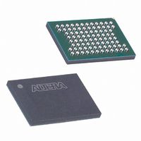
Manufacturer Part Number
EPC16UC88
Description
IC CONFIG DEVICE 16MBIT 88-UBGA
Manufacturer
Altera
Series
EPCr
Datasheet
1.EPC8QC100.pdf
(34 pages)
Specifications of EPC16UC88
Programmable Type
In System Programmable
Memory Size
16Mb
Voltage - Supply
3 V ~ 3.6 V
Operating Temperature
0°C ~ 70°C
Package / Case
88-UBGA
Lead Free Status / RoHS Status
Contains lead / RoHS non-compliant
Other names
544-1228
Available stocks
Company
Part Number
Manufacturer
Quantity
Price
Company:

Part Number:
EPC16UC88
Manufacturer:
ALTERA
Quantity:
62
Company:
Part Number:
EPC16UC88
Manufacturer:
ALTERA
Quantity:
275
Part Number:
EPC16UC88
Manufacturer:
ALTERA/阿尔特拉
Quantity:
20 000
Company:
Part Number:
EPC16UC888N
Manufacturer:
ALTERA
Quantity:
621
Company:
Part Number:
EPC16UC88AA
Manufacturer:
ALTERA
Quantity:
280
Part Number:
EPC16UC88AA
Manufacturer:
ALTERA
Quantity:
20 000
Part Number:
EPC16UC88N
Manufacturer:
ALTERA/阿尔特拉
Quantity:
20 000


1–16
Configuration Handbook (Complete Two-Volume Set)
1
1
2. Using V
3. Using a high CE# disables the chip. The requirement for a write is a low CE# and
4. Using a high WE# prevent writes because a write only occurs when the WE# is low.
Performing all four methods simultaneously is the safest protection for the flash
content.
The ideal power-up sequence is as follows:
1. Power-up V
2. Maintain V
3. Power-up V
4. Drive RP# low during the entire power-up process. RP# must be released high
CE# and WE# must be high for the entire power-up sequence.
The ideal power-down sequence is as follows:
1. Drive RP# low for 100ns before power-down.
2. Power-down V
3. Power-down V
4. Drive RP# low during the entire power-down process.
CE# and WE# must be high for the entire power-down sequence.
The RP# pin is not internally connected to the controller. Therefore, an external
loop-back connection between C-RP# and F-RP# must be made on the board even
when you are not using the external device to the RP# pin with the loop-back. Always
tri-state RP# when the flash is not in use.
If an external power-up monitoring circuit is connected to the RP# pin with the
loop-back, use the following guidelines to avoid contention on the RP# line:
■
■
If the preceding guidelines cannot be completed within 50 ms, then the OE pin must
be driven low externally until RP# is ready to be released.
V
supply voltage input pin on the Intel flash. V
EPC devices.
low WE#. A high CE# by itself prevents writes from occurring.
within 25 ms after V
The power-up sequence on the 3.3-V supply should complete within 50 ms of
power-up. The 3.3-V V
should then be released.
RP# should be driven low by the power-up monitoring circuit during power-up.
After power-up, RP# should be tri-stated externally by the power-up monitoring
circuit.
PP
< V
PPLK
PP
< V
PP
means programming or writes cannot occur. V
CC
PP
< V
PPLK
.
.
PP
CC
PPLK
.
< V
, where the maximum value of V
PP
PPLK
until V
Chapter 1: Enhanced Configuration Devices (EPC4, EPC8, and EPC16) Data Sheet
is powered up.
CC
.
should reach the minimum V
CC
is fully powered up.
PP
is equivalent to the VCCW pin on
PPLK
© December 2009 Altera Corporation
CC
is 1 V, disables writes.
before 50 ms and RP#
PP
is a programming
Functional Description
Related parts for EPC16UC88
Image
Part Number
Description
Manufacturer
Datasheet
Request
R

Part Number:
Description:
Configuration Devices
Manufacturer:
Altera Corporation
Datasheet:

Part Number:
Description:
IC CONFIG DEVICE 1MBIT 8-DIP
Manufacturer:
Altera
Datasheet:

Part Number:
Description:
IC CONFIG DEVICE 1.6MBIT 20-PLCC
Manufacturer:
Altera
Datasheet:
Part Number:
Description:
IC CONFIG DEVICE 1.6MBIT 20-PLCC
Manufacturer:
Altera
Datasheet:

Part Number:
Description:
IC CONFIG DEVICE 1.6MBIT 32-TQFP
Manufacturer:
Altera
Datasheet:
Part Number:
Description:
IC CONFIG DEVICE 1.6MBIT 32-TQFP
Manufacturer:
Altera
Datasheet:
Part Number:
Description:
IC CONFIG DEVICE 1.6MBIT 20-PLCC
Manufacturer:
Altera
Datasheet:
Part Number:
Description:
IC CONFIG DEVICE 1.6MBIT 20-PLCC
Manufacturer:
Altera
Datasheet:

Part Number:
Description:
IC CONFIG DEVICE 8MBIT 100-PQFP
Manufacturer:
Altera
Datasheet:
Part Number:
Description:
IC CONFIG DEVICE 1.6MBIT 32-TQFP
Manufacturer:
Altera
Datasheet:
Part Number:
Description:
IC CONFIG DEVICE 1.6MBIT 32-TQFP
Manufacturer:
Altera
Datasheet:
Part Number:
Description:
IC CONFIG DEVICE 16MBIT 100-PQFP
Manufacturer:
Altera
Datasheet:
Part Number:
Description:
IC CONFIG DEVICE 16MBIT 100-PQFP
Manufacturer:
Altera
Datasheet:
Part Number:
Description:
IC CONFIG DEVICE 16MBIT 100-PQFP
Manufacturer:
Altera
Datasheet:

Part Number:
Description:
IC CONFIG DEVICE 16MBIT 88-UBGA
Manufacturer:
Altera
Datasheet: