AT17LV128-10JC Atmel, AT17LV128-10JC Datasheet - Page 8
AT17LV128-10JC
Manufacturer Part Number
AT17LV128-10JC
Description
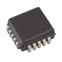
IC SER CFG PROM 128K 3.3V 20PLCC
Manufacturer
Atmel
Datasheet
1.AT17LV65-10CC.pdf
(26 pages)
Specifications of AT17LV128-10JC
Programmable Type
Serial EEPROM
Memory Size
128kb
Voltage - Supply
3 V ~ 3.6 V, 4.75 V ~ 5.25 V
Operating Temperature
0°C ~ 70°C
Package / Case
20-LCC (J-Lead)
For Use With
ATDH2225 - CABLE ISP FOR AT17ATDH2200E - CONFIGURATOR PROGRAM BOARD KIT
Lead Free Status / RoHS Status
Contains lead / RoHS non-compliant
Available stocks
Company
Part Number
Manufacturer
Quantity
Price

Part Number:
AT17LV128-10JC
Manufacturer:
ATMEL/爱特梅尔
Quantity:
20 000


4.10
4.11
4.12
4.13
5. FPGA Master Serial Mode Summary
6. Control of Configuration
8
A2
READY
SER_EN
V
AT17LV65/128/256/512/010/002/040
CC
Device selection input, A2. This is used to enable (or select) the device during programming
(i.e., when SER_EN is Low). A2 has an internal pull-down resistor.
Open collector reset state indicator. Driven Low during power-up reset, released when power-up
is complete. It is recommended to use a 4.7 kΩ pull-up resistor when this pin is used.
Serial enable must be held High during FPGA loading operations. Bringing SER_EN Low
enables the Two-Wire Serial Programming Mode. For non-ISP applications, SER_EN should be
tied to V
3.3V (±10%) and 5.0V (±5% Commercial, ±10% Industrial) power supply pin.
The I/O and logic functions of any SRAM-based FPGA are established by a configuration pro-
gram. The program is loaded either automatically upon power-up, or on command, depending
on the state of the FPGA mode pins. In Master mode, the FPGA automatically loads the config-
uration program from an external memory. The AT17LV Serial Configuration EEPROM has
been designed for compatibility with the Master Serial mode.
This document discusses the Atmel AT40K, AT40KAL and AT94KAL applications as well as Xil-
inx applications.
Most connections between the FPGA device and the AT17LV Serial EEPROM are simple and
self-explanatory.
Note:
• The DATA output of the AT17LV series configurator drives DIN of the FPGA devices.
• The master FPGA CCLK output drives the CLK input of the AT17LV series configurator.
• The CEO output of any AT17LV series configurator drives the CE input of the next
• SER_EN must be connected to V
• The READY
configurator in a cascaded chain of EEPROMs.
driven Low while the device is in its power-on reset cycle and released (tri-stated) when the
cycle is complete.
1. This pin is not available for the AT17LV65/128/256 devices.
CC
.
(1)
pin is available as an open-collector indicator of the device’s reset status; it is
CC
(except during ISP).
2321I–CNFG–2/08
Related parts for AT17LV128-10JC
Image
Part Number
Description
Manufacturer
Datasheet
Request
R

Part Number:
Description:
Manufacturer:
ATMEL Corporation
Datasheet:

Part Number:
Description:
IC SRL CONFIG EEPROM 128K 20SOIC
Manufacturer:
Atmel
Datasheet:

Part Number:
Description:
IC SRL CONFIG EEPROM 128K 8-DIP
Manufacturer:
Atmel
Datasheet:

Part Number:
Description:
IC SRL CONFIG EEPROM 128K 8-LAP
Manufacturer:
Atmel
Datasheet:
Part Number:
Description:
IC SRL CONFG EEPROM 128K LV 8LAP
Manufacturer:
Atmel
Datasheet:

Part Number:
Description:
IC EEPROM FPGA 128KB 8-SOIC
Manufacturer:
Atmel
Datasheet:
Part Number:
Description:
IC EEPROM FPGA 128KB 8-SOIC
Manufacturer:
Atmel
Datasheet:
Part Number:
Description:
IC SRL CONFIG EEPROM 128K 20SOIC
Manufacturer:
Atmel
Datasheet:
Part Number:
Description:
IC SER CNFIG PROM 128K 3.3V 8DIP
Manufacturer:
Atmel
Datasheet:

Part Number:
Description:
IC EEPROM FPGA 128KB 20-PLCC
Manufacturer:
Atmel
Datasheet:

Part Number:
Description:
Memory - FPGA Configuration FPGA CONFIG SERIAL EEPROM, 128K, 3.3V - DIE WAFER
Manufacturer:
Atmel

Part Number:
Description:
DEV KIT FOR AVR/AVR32
Manufacturer:
Atmel
Datasheet:
Part Number:
Description:
INTERVAL AND WIPE/WASH WIPER CONTROL IC WITH DELAY
Manufacturer:
ATMEL Corporation
Datasheet:
Part Number:
Description:
Low-Voltage Voice-Switched IC for Hands-Free Operation
Manufacturer:
ATMEL Corporation
Datasheet: