TOP258GN-TL Power Integrations, TOP258GN-TL Datasheet - Page 6
TOP258GN-TL
Manufacturer Part Number
TOP258GN-TL
Description
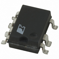
IC OFFLINE SWIT PROG OVP 8SMD
Manufacturer
Power Integrations
Series
TOPSwitch®-HXr
Type
Off Line Switcherr
Datasheet
1.TOP252GN-TL.pdf
(48 pages)
Specifications of TOP258GN-TL
Output Isolation
Isolated
Frequency Range
119 ~ 145kHz
Voltage - Output
700V
Power (watts)
77W
Operating Temperature
-40°C ~ 150°C
Package / Case
8-SMD Gull Wing, 7 Leads
Output Voltage
700 V
Input / Supply Voltage (max)
9 V
Input / Supply Voltage (min)
- 0.3 V
Duty Cycle (max)
78 %
Switching Frequency
132 KHz
Operating Temperature Range
- 40 C to + 150 C
Mounting Style
SMD/SMT
Maximum Operating Temperature
+ 150 C
Minimum Operating Temperature
- 40 C
Output Current
6.88 A
Output Power
48 W
For Use With
596-1193 - KIT REF DESIGN TOP HX FOR TOP258
Lead Free Status / RoHS Status
Lead free / RoHS Compliant
Other names
596-1190-2
Available stocks
Company
Part Number
Manufacturer
Quantity
Price

Part Number:
TOP258GN-TL
Manufacturer:
POWER
Quantity:
20 000


Pin Functional Description
DRAIN (D) Pin:
High-voltage power MOSFET DRAIN pin. The internal start-up
bias current is drawn from this pin through a switched high-
voltage current source. Internal current limit sense point for
drain current.
CONTROL (C) Pin:
Error amplifi er and feedback current input pin for duty cycle
control. Internal shunt regulator connection to provide internal
bias current during normal operation. It is also used as the
connection point for the supply bypass and auto-restart/
compensation capacitor.
EXTERNAL CURRENT LIMIT (X) Pin (Y, M, E and L package):
Input pin for external current limit adjustment and remote
ON/OFF. A connection to SOURCE pin disables all functions
on this pin.
Figure 4.
Rev. F 01/09
6
M
X
C
C
D
V
D
E Package (eSIP-7C)
L Package (eSIP-7F)
P and G Package
4
2
5
1
1
2
3
Pin Confi guration (Top View).
V
V
1
1
M Package
TOP252-262
X
X
2
2
C
C
3
3
F
F
4
4
S
5
5
S
D
D
7
7
10
9
8
7
6
8
7
6
5
Exposed Pad
(Hidden)
Internally
Connected to
SOURCE Pin
S
S
S
S
S
S
S
S
S
Lead Bend
Outward from Drawing
(Refer to eSIP-7F Package
Outline Drawing)
Tab Internally
Connected to
SOURCE Pin
Tab Internally
Connected to
SOURCE Pin
Note: Y package for TOP259-261
Note: Y package for TOP254-258
Y Package (TO-220-7C)
Y Package (TO-220-7C)
V
1
V
1
X
2
X
2
C
3
C
3
S
4
S
4
G
5
5
F
PI-4644-091108
D
7
D
7
VOLTAGE MONITOR (V) Pin (Y & M package only):
Input for OV, UV, line feed forward with DC
overvoltage protection (OVP), remote ON/OFF and device reset.
A connection to the SOURCE pin disables all functions on this pin.
MULTI-FUNCTION (M) Pin (P & G packages only):
This pin combines the functions of the VOLTAGE MONITOR (V)
and EXTERNAL CURRENT LIMIT (X) pins of the Y package into
one pin. Input pin for OV, UV, line feed forward with DC
Figure 5.
Figure 6.
Figure 7.
Voltage
Voltage
Voltage
Input
Input
Input
TOP254-258 Y and All M/E/L Package Line Sense and Externally Set
Current Limit.
TOP259-261 Y Package Line Sense and External Current Limit.
P/G Package Line Sense.
DC
DC
DC
+
+
+
-
-
-
D
S
D
S
D
S
12 k
R
R
R
R
CONTROL
CONTROL
CONTROL
LS
LS
LS
IL
X
X
12 k
R
V
V
M
IL
4 M
4 M
4 M
G
V
V
For R
DC
DC
C
C
C
V
V
DC
DC
V
V
DC
DC
For R
For R
UV
OV
UV
OV
UV
OV
MAX
MAX
MAX
MAX
MAX
MAX
V
V
For R
For R
= I
MAX
= I
= I
= I
V
V
= I
= I
V
V
See Figure 55b for
other resistor values
(R
I
See Figure 55b for
other resistor values
(R
I
UV
OV
LS
LIMIT
LIMIT
I
I
LS
UV
OV
LS
UV
OV
@100 VDC = 76%
@375 VDC = 41%
LIMIT
LIMIT
UV
OV
@100 VDC = 76%
@375 VD
@100 VDC = 76%
@375 VD
UV
OV
UV
OV
IL
IL
= 4 M
= 102.8 VDC
= 451 VDC
www.powerint.com
reduction, output
) to select different
) to select different
= 4 M
= 4 M
= 102.8 VDC
= 451 VDC
= 102.8 VDC
= 451 VDC
IL
IL
× R
× R
× R
× R
× R
× R
values.
values.
= 12 k
= 12 k
= 61%
= 61%
LS
LS
LS
LS
LS
LS
+ V
+ V
+ V
+ V
PI-4712-120307
+ V
+ V
C = 41%
C = 41%
M
M
V
V
V
V
MAX
(I
(I
(I
(I
(I
(I
M
V
V
M
V
V
= I
= I
= I
= I
= I
= I
UV
UV
UV
OV
OV
OV
)
)
)
)
)
)
Related parts for TOP258GN-TL
Image
Part Number
Description
Manufacturer
Datasheet
Request
R

Part Number:
Description:
SOP-16
Manufacturer:
Power Integrations
Datasheet:
Part Number:
Description:
DIP8
Manufacturer:
Power Integrations
Datasheet:
Part Number:
Description:
TO-263
Manufacturer:
Power Integrations
Datasheet:
Part Number:
Description:
TO-263
Manufacturer:
Power Integrations
Datasheet:
Part Number:
Description:
Manufacturer:
Power Integrations
Datasheet: