TOP222YN Power Integrations, TOP222YN Datasheet - Page 6
TOP222YN
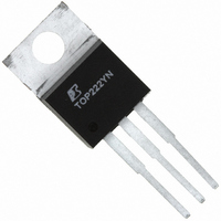
Manufacturer Part Number
TOP222YN
Description
IC OFFLINE SWIT PWM OCP HV TO220
Manufacturer
Power Integrations
Series
TOPSwitch®-IIr
Type
Off Line Switcherr
Datasheet
1.TOP222GN-TL.pdf
(20 pages)
Specifications of TOP222YN
Output Isolation
Isolated
Frequency Range
90 ~ 110kHz
Voltage - Output
700V
Power (watts)
25W
Operating Temperature
-40°C ~ 150°C
Package / Case
TO-220-3
Output Voltage
5.7 V
Input / Supply Voltage (max)
265 VAC
Input / Supply Voltage (min)
85 VAC
Duty Cycle (max)
70 %
Switching Frequency
100 KHz
Supply Current
1.2 mA
Operating Temperature Range
- 40 C to + 150 C
Mounting Style
Through Hole
Lead Free Status / RoHS Status
Lead free / RoHS Compliant
Other names
596-1156-5
TOP222YN
TOP222YN
Available stocks
Company
Part Number
Manufacturer
Quantity
Price
Company:

Part Number:
TOP222YN
Manufacturer:
PI
Quantity:
2 650
Company:
Part Number:
TOP222YN
Manufacturer:
MT
Quantity:
5 510
Part Number:
TOP222YN
Manufacturer:
POWER
Quantity:
20 000


Figure 7. Schematic Diagram of a 4 W TOPSwitch-II Standby Power Supply using an 8 lead PDIP.
Application Examples
Following are just two of the many possible TOPSwitch
implementations. Refer to the Data Book and Design Guide
for additional examples.
4 W Standby Supply using 8 Lead PDIP
Figure 7 shows a 4 W standby supply. This supply is used in
appliances where certain standby functions (e.g. real time
clock, remote control port) must be kept active even while the
main power supply is turned off.
The 5 V secondary is used to supply the standby function and
the 12 V non-isolated output is used to supply power for the
PWM controller of the main power supply and other primary
side functions.
For this application the input rectifiers and input filter are sized
for the main supply and are not shown. The input DC rail may
6
TOP221-227
D
7/01
Wide-Range
DC Input
+
-
47 k
R3
UF4005
D1
D
S
TOP221P
2.2 nF
CONTROL
1 kV
C1
U1
C
TOPSwitch-II
T1
UF5401
D2
vary from 100 V to 380 V DC which corresponds to the full
universal AC input range. The TOP221 is packaged in an 8 pin
power DIP package.
The output voltage (5 V) is directly sensed by the Zener diode
(VR1) and the optocoupler (U2). The output voltage is determined
by the sum of the Zener voltage and the voltage drop across the
LED of the optocoupler (the voltage drop across R1 is negligible).
The output transistor of the optocoupler drives the CONTROL
pin of the TOP221. C5 bypasses the CONTROL pin and provides
control loop compensation and sets the auto-restart frequency.
The transformer’s leakage inductance voltage spikes are snubbed
by R3 and C1 through diode D1. The bias winding is rectified
and filtered by D3 and C4 providing a non-isolated 12 V output
which is also used to bias the collector of the optocoupler’s
output transistor. The isolated 5 V output winding is rectified by
D2 and filtered by C2, L1 and C3.
330 F
1N4148
100 F
10 V
C2
47 F
16 V
10 V
C4
D3
C5
PC817A
VR1
10
R1
U2
100
3.3 H
R2
L1
100 F
10 V
C3
+
12 V Non-Isolated
-
+5 V
RTN
PI-2115-040401
Related parts for TOP222YN
Image
Part Number
Description
Manufacturer
Datasheet
Request
R

Part Number:
Description:
SOP-16
Manufacturer:
Power Integrations
Datasheet:
Part Number:
Description:
DIP8
Manufacturer:
Power Integrations
Datasheet:
Part Number:
Description:
TO-263
Manufacturer:
Power Integrations
Datasheet:
Part Number:
Description:
TO-263
Manufacturer:
Power Integrations
Datasheet:
Part Number:
Description:
Manufacturer:
Power Integrations
Datasheet: