LNK353GN Power Integrations, LNK353GN Datasheet - Page 6
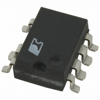
LNK353GN
Manufacturer Part Number
LNK353GN
Description
IC OFFLINE SWIT OCP HV 8SMD
Manufacturer
Power Integrations
Series
LinkSwitch®-HFr
Type
Off Line Switcherr
Datasheet
1.LNK353GN-TL.pdf
(16 pages)
Specifications of LNK353GN
Output Isolation
Isolated
Frequency Range
186 ~ 214kHz
Voltage - Output
700V
Power (watts)
4W
Operating Temperature
-40°C ~ 150°C
Package / Case
8-SMD Gull Wing, 7 Leads
Output Voltage
5.8 V
Input / Supply Voltage (max)
265 VAC
Input / Supply Voltage (min)
85 VAC
Duty Cycle (max)
63 %
Switching Frequency
200 KHz
Supply Current
280 uA
Operating Temperature Range
- 40 C to + 150 C
Mounting Style
SMD/SMT
Lead Free Status / RoHS Status
Lead free / RoHS Compliant
Other names
596-1172
LNK353GN
LNK353GN
Available stocks
Company
Part Number
Manufacturer
Quantity
Price

Part Number:
LNK353GN-TL
Manufacturer:
POWER
Quantity:
20 000


of the diode for heatsinking. A larger area is preferred at the
quiet cathode terminal. A large anode area can increase high
frequency radiated EMI.
Quick Design Checklist
As with any power supply design, all LinkSwitch-HF designs
should be verified on the bench to make sure that component
specifications are not exceeded under worst-case conditions. The
following minimum set of tests is strongly recommended:
1. Maximum drain voltage – Verify that V
2. Maximum drain current – At maximum ambient temperature,
Figure 6. Recommended Printed Circuit Layout for LinkSwitch-HF in a Flyback Converter Configuration.
HV DC
6
Input
675 V at the highest input voltage and peak (overload) output
power.
maximum input voltage and peak output (overload) power,
verify drain current waveforms for any signs of transformer
saturation and excessive leading edge current spikes at
startup. Repeat under steady state conditions and verify that
LNK353/354
+
-
F
2/05
TOP VIEW
S
S
LinkSwitch-HF
S
S
DS
C
BP
does not exceed
Input Filter
BP
Capacitor
D
FB
PRI
3. Thermal Check – At specified maximum output power,
Design Tools
Up-to-date information on design tools can be found at the
Power Integrations website: www.powerint.com.
the leading edge current spike event is below I
end of the t
current should be below the specified absolute maximum
ratings.
minimum input voltage and maximum ambient temperature,
verify that the temperature specifications are not exceeded
for LinkSwitch-HF, transformer, output diode, and output
capacitors. Enough thermal margin should be allowed for
part-to-part variation of the R
specified in the data sheet. Under low line, maximum power,
a maximum LinkSwitch-HF SOURCE pin temperature of
100 °C is recommended to allow for these variations.
coupler
Capacitor
Opto-
Y1-
m
T
a
n
s
o
e
r
r
r
f
LEB(MIN)
SEC
. Under all conditions, the maximum drain
Maximize hatched copper
areas (
heatsinking
DS(ON)
of LinkSwitch-HF as
Output Filter
) for optimum
Capacitor
PI-3890-102704
LIMIT(MIN)
at the
Out
DC
+
-
Related parts for LNK353GN
Image
Part Number
Description
Manufacturer
Datasheet
Request
R

Part Number:
Description:
Enhanced, Energy Efficient, Low Power Off-Line Switcher IC
Manufacturer:
POWERINT [Power Integrations, Inc.]
Datasheet:

Part Number:
Description:
SOP-16
Manufacturer:
Power Integrations
Datasheet:
Part Number:
Description:
DIP8
Manufacturer:
Power Integrations
Datasheet:
Part Number:
Description:
TO-263
Manufacturer:
Power Integrations
Datasheet:
Part Number:
Description:
TO-263
Manufacturer:
Power Integrations
Datasheet: