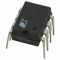
TOP209P Power Integrations, TOP209P Datasheet - Page 4

TOP209P
Manufacturer Part Number
TOP209P
Description
IC OFFLINE SWIT PWM OCP HV 8DIP
Manufacturer
Power Integrations
Series
TOPSwitch®r
Type
Off Line Switcherr
Datasheet
1.TOP210PN.pdf
(16 pages)
Specifications of TOP209P
Output Isolation
Isolated
Frequency Range
55 ~ 85kHz
Voltage - Output
700V
Power (watts)
2W
Operating Temperature
-40°C ~ 150°C
Package / Case
8-DIP (0.300", 7.62mm)
Output Voltage
5.8 V
Input / Supply Voltage (max)
265 VAC
Input / Supply Voltage (min)
85 VAC
Duty Cycle (max)
70 %
Switching Frequency
70 KHz
Supply Current
1.2 mA
Operating Temperature Range
- 40 C to + 150 C
Mounting Style
Through Hole
Lead Free Status / RoHS Status
Contains lead / RoHS non-compliant
Available stocks
Company
Part Number
Manufacturer
Quantity
Price
Company:
Part Number:
TOP209P
Manufacturer:
MICROELE
Quantity:
6 000
Part Number:
TOP209P
Manufacturer:
PI
Quantity:
20 000
Company:
Part Number:
TOP209PFI
Manufacturer:
POWER
Quantity:
15 000
Part Number:
TOP209PFI
Manufacturer:
POWER
Quantity:
20 000
Company:
Part Number:
TOP209PN
Manufacturer:
POWER
Quantity:
15 000
Part Number:
TOP209PN
Manufacturer:
POWER
Quantity:
20 000
2
TOPSwitch Family Functional Description (cont.)
The first time V
current source is turned off and the PWM modulator and output
transistor are activated, as shown in Figure 5(a). During normal
operation (when the output voltage is regulated) feedback
control current supplies the V
regulator keeps V
pin feedback current exceeding the required DC supply current
through the PWM error signal sense resistor R
dynamic impedance of this pin (Z
amplifier when used in a primary feedback configuration. The
dynamic impedance of the CONTROL pin together with the
external resistance and capacitance determines the control loop
compensation of the power system.
If the CONTROL pin external capacitance (C
to the lower threshold, then the output MOSFET is turned off
and the control circuit is placed in a low-current standby mode.
The high-voltage current source is turned on and charges the
external capacitance again. Charging current is shown with a
negative polarity and discharging current is shown with a
positive polarity in Figure 6. The hysteretic auto-restart
comparator keeps V
by turning the high-voltage current source on and off as shown
in Figure 5(b). The auto-restart circuit has a divide-by-8
counter which prevents the output MOSFET from turning on
again until eight discharge-charge cycles have elapsed. The
counter effectively limits TOPSwitch power dissipation by
reducing the auto-restart duty cycle to typically 5%. Auto-
restart continues to cycle until output voltage regulation is
again achieved.
Bandgap Reference
All critical TOPSwitch internal voltages are derived from a
temperature-compensated bandgap reference. This reference
is also used to generate a temperature-compensated current
source which is trimmed to accurately set the oscillator frequency
and MOSFET gate drive current.
Oscillator
The internal oscillator linearly charges and discharges the
internal capacitance between two voltage levels to create a
sawtooth waveform for the pulse width modulator. The oscillator
sets the pulse width modulator/current limit latch at the beginning
of each cycle. The nominal frequency of 100 kHz was chosen
to minimize EMI and maximize efficiency in power supply
applications. Trimming of the current reference improves
oscillator frequency accuracy.
Pulse Width Modulator
The pulse width modulator implements a voltage-mode control
4
TOP209/210
A
8/97
C
reaches the upper threshold, the high-voltage
C
at typically 5.7 V by shunting CONTROL
C
within a window of typically 4.7 to 5.7 V
C
supply current. The shunt
C
) sets the gain of the error
T
) should discharge
E
. The low
loop by driving the output MOSFET with a duty cycle inversely
proportional to the current flowing into the CONTROL pin.
The error signal across R
typical corner frequency of 7 kHz to reduce the effect of
switching noise. The filtered error signal is compared with the
internal oscillator sawtooth waveform to generate the duty
cycle waveform. As the control current increases, the duty
cycle decreases. A clock signal from the oscillator sets a latch
which turns on the output MOSFET. The pulse width modulator
resets the latch, turning off the output MOSFET. The maximum
duty cycle is set by the symmetry of the internal oscillator. The
modulator has a minimum ON-time to keep the current
consumption of the TOPSwitch independent of the error signal.
Note that a minimum current must be driven into the CONTROL
pin before the duty cycle begins to change.
Gate Driver
The gate driver is designed to turn the output MOSFET on at a
controlled rate to minimize common-mode EMI. The gate drive
current is trimmed for improved accuracy.
Error Amplifier
The shunt regulator can also perform the function of an error
amplifier in primary feedback applications. The shunt regulator
voltage is accurately derived from the temperature compensated
bandgap reference. The gain of the error amplifier is set by the
CONTROL pin dynamic impedance. The CONTROL pin
clamps external circuit signals to the V
CONTROL pin current in excess of the supply current is
separated by the shunt regulator and flows through R
error signal.
Cycle-By-Cycle Current Limit
The cycle by cycle peak drain current limit circuit uses the
output MOSFET ON-resistance as a sense resistor. A current
limit comparator compares the output MOSFET ON-state drain-
source voltage, V
current causes V
the output MOSFET off until the start of the next clock cycle.
The current limit comparator threshold voltage is temperature
compensated to minimize variation of the effective peak current
limit due to temperature related changes in output MOSFET
R
The leading edge blanking circuit inhibits the current limit
comparator for a short time after the output MOSFET is turned
on. The leading edge blanking time has been set so that current
spikes caused by primary-side capacitances and secondary-side
rectifier reverse recovery time will not cause premature
termination of the switching pulse.
DS(ON)
.
DS(ON)
DS(ON)
to exceed the threshold voltage and turns
, with a threshold voltage. High drain
E
is filtered by an RC network with a
C
voltage level. The
E
as the


