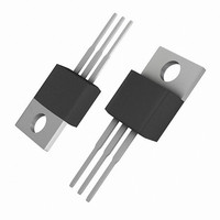
TOP223Y Power Integrations, TOP223Y Datasheet - Page 2

TOP223Y
Manufacturer Part Number
TOP223Y
Description
IC OFFLINE SWIT PWM OCP HV TO220
Manufacturer
Power Integrations
Series
TOPSwitch®-IIr
Type
Off Line Switcherr
Datasheet
1.TOP222GN-TL.pdf
(20 pages)
Specifications of TOP223Y
Output Isolation
Isolated
Frequency Range
90 ~ 110kHz
Voltage - Output
700V
Power (watts)
50W
Operating Temperature
-40°C ~ 150°C
Package / Case
TO-220-3
Output Voltage
5.7 V
Input / Supply Voltage (max)
265 VAC
Input / Supply Voltage (min)
85 VAC
Duty Cycle (max)
70 %
Switching Frequency
100 KHz
Supply Current
1.2 mA
Operating Temperature Range
- 40 C to + 150 C
Mounting Style
Through Hole
Lead Free Status / RoHS Status
Contains lead / RoHS non-compliant
Available stocks
Company
Part Number
Manufacturer
Quantity
Price
Company:
Part Number:
TOP223Y
Manufacturer:
POWER
Quantity:
4 137
Company:
Part Number:
TOP223Y
Manufacturer:
POWERINTE
Quantity:
224
Part Number:
TOP223Y
Manufacturer:
POWER
Quantity:
20 000
Company:
Part Number:
TOP223YAL
Manufacturer:
POWER
Quantity:
2 500
Company:
Part Number:
TOP223YN
Manufacturer:
PowerInt
Quantity:
3 250
Part Number:
TOP223YN
Manufacturer:
POWER
Quantity:
20 000
Figure 2. Functional Block Diagram.
Pin Functional Description
DRAIN Pin:
Output MOSFET drain connection. Provides internal bias
current during start-up operation via an internal switched high-
voltage current source. Internal current sense point.
CONTROL Pin:
Error amplifier and feedback current input pin for duty cycle
control. Internal shunt regulator connection to provide internal
bias current during normal operation. It is also used as the
connection point for the supply bypass and auto-restart/
compensation capacitor.
SOURCE Pin:
Y package – Output MOSFET source connection for high
P and G package – Primary side control circuit common and
SOURCE (HV RTN) Pin: (P and G package only)
Output MOSFET source connection for high voltage power return.
2
CONTROL
TOP221-227
D
7/01
voltage power return. Primary side circuit
common and reference point.
reference point.
R E
Z C
I FB
SHUNT REGULATOR/
ERROR AMPLIFIER
OSCILLATOR
V C
CLOCK
D MAX
SAW
+
-
5.7 V
SHUTDOWN
COMPARATOR
5.7 V
4.7 V
THERMAL
PWM
-
+
AUTO-RESTART
SHUTDOWN/
+
-
POWER-UP
RESET
0
1
INTERNAL
SUPPLY
S
R
Figure 3. Pin Configuration.
8
Q
Q
S
R
Connected to SOURCE Pin
CONTROL
Q
Q
SOURCE
SOURCE
SOURCE
Tab Internally
Y Package (TO-220/3)
G Package (SMD-8)
P Package (DIP-8)
2
1
3
4
BLANKING
LEADING
EDGE
CONTROLLED
TURN-ON
DRIVER
GATE
8
6
5
7
+
-
SOURCE (HV RTN)
SOURCE (HV RTN)
SOURCE (HV RTN)
DRAIN
MINIMUM
ON-TIME
DELAY
V I
LIMIT
DRAIN
SOURCE
CONTROL
PI-2084-040401
PI-1935-091696
DRAIN
SOURCE


