TOP223Y Power Integrations, TOP223Y Datasheet - Page 3
TOP223Y
Manufacturer Part Number
TOP223Y
Description
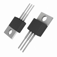
IC OFFLINE SWIT PWM OCP HV TO220
Manufacturer
Power Integrations
Series
TOPSwitch®-IIr
Type
Off Line Switcherr
Datasheet
1.TOP222GN-TL.pdf
(20 pages)
Specifications of TOP223Y
Output Isolation
Isolated
Frequency Range
90 ~ 110kHz
Voltage - Output
700V
Power (watts)
50W
Operating Temperature
-40°C ~ 150°C
Package / Case
TO-220-3
Output Voltage
5.7 V
Input / Supply Voltage (max)
265 VAC
Input / Supply Voltage (min)
85 VAC
Duty Cycle (max)
70 %
Switching Frequency
100 KHz
Supply Current
1.2 mA
Operating Temperature Range
- 40 C to + 150 C
Mounting Style
Through Hole
Lead Free Status / RoHS Status
Contains lead / RoHS non-compliant
Available stocks
Company
Part Number
Manufacturer
Quantity
Price
Company:

Part Number:
TOP223Y
Manufacturer:
POWER
Quantity:
4 137
Company:
Part Number:
TOP223Y
Manufacturer:
POWERINTE
Quantity:
224
Part Number:
TOP223Y
Manufacturer:
POWER
Quantity:
20 000
Company:
Part Number:
TOP223YAL
Manufacturer:
POWER
Quantity:
2 500
Company:
Part Number:
TOP223YN
Manufacturer:
PowerInt
Quantity:
3 250
Part Number:
TOP223YN
Manufacturer:
POWER
Quantity:
20 000


TOPSwitch-II Family Functional Description
TOPSwitch is a self biased and protected linear control current-
to-duty cycle converter with an open drain output. High
efficiency is achieved through the use of CMOS and integration
of the maximum number of functions possible. CMOS process
significantly reduces bias currents as compared to bipolar or
discrete solutions. Integration eliminates external power
resistors used for current sensing and/or supplying initial start-
up bias current.
During normal operation, the duty cycle of the internal output
MOSFET decreases linearly with increasing CONTROL pin
current as shown in Figure 4. To implement all the required
control, bias, and protection functions, the DRAIN and
CONTROL pins each perform several functions as described
below. Refer to Figure 2 for a block diagram and to Figure 6 for
timing and voltage waveforms of the TOPSwitch integrated
circuit.
Figure 5. Start-up Waveforms for (a) Normal Operation and (b) Auto-restart.
DRAIN
DRAIN
V C
V C
5.7 V
4.7 V
5.7 V
4.7 V
V IN
V IN
0
0
0
0
Charging C T
Charging C T
C
T
connected to the CONTROL pin
Off
Off
I C
I C
is the total external capacitance
Switching
(a)
(b)
Discharging C T
Figure 4. Relationship of Duty Cycle to CONTROL Pin Current.
Off
I CD1
95%
8 Cycles
D MAX
D MIN
Switching
Auto-restart
I CD1
Switching
5%
2.0
Discharging C T
I B
I CD2
Off
I C (mA)
Slope = PWM Gain
TOP221-227
6.0
PI-1956-092496
7/01
PI-2040-050197
D
3
Related parts for TOP223Y
Image
Part Number
Description
Manufacturer
Datasheet
Request
R

Part Number:
Description:
IC OFFLINE CTRLR SMPS CM TO220
Manufacturer:
Infineon Technologies
Datasheet:

Part Number:
Description:
IC OFFLINE CTRLR SMPS CM TO220
Manufacturer:
Infineon Technologies
Datasheet:

Part Number:
Description:
SOP-16
Manufacturer:
Power Integrations
Datasheet:
Part Number:
Description:
DIP8
Manufacturer:
Power Integrations
Datasheet:
Part Number:
Description:
TO-263
Manufacturer:
Power Integrations
Datasheet: