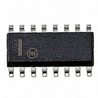
NCP1205DR2 ON Semiconductor, NCP1205DR2 Datasheet

NCP1205DR2
Specifications of NCP1205DR2
Available stocks
Related parts for NCP1205DR2
NCP1205DR2 Summary of contents
Page 1
... Pb--Free Package ORDERING INFORMATION Device Package NCP1205PG PDIP--8 (Pb--Free) NCP1205P2G PDIP--14 (Pb--Free) NCP1205DR2G SOIC--16 (Pb--Free) †For information on tape and reel specifications, including part orientation and tape sizes, please refer to our Tape and Reel Packaging Specifications Brochure, BRD8011/D. 1 MARKING DIAGRAM ...
Page 2
Demag 2 7 Drive Isense GND PDIP- -8 PIN FUNCTION DESCRIPTION Pin No. PDIP- -8 PDIP- -14 SOIC- -16 Pin Name Demag ...
Page 3
4x1N4007 Universal Input R6 4 Please refer to the application information section regarding this element. Figure 1. Typical Application Example for PDIP- -8 Version + 4x1N4007 ...
Page 4
HV 1 Last Pulse of Demag after DEMAG ? Demag 2 Over Current Protection (OCP) V(--) < 1.5 V Lasts more than 128 ms? ...
Page 5
HV 1 Last Pulse of Demag after DEMAG ? Demag 2 OVP 6 Over Current Protection (OCP) V(--) < 1 ...
Page 6
MAXIMUM RATINGS Rating Power Supply Voltage Thermal Resistance Junction--to--Air Operating Junction Temperature Range Maximum Junction Temperature Storage Temperature Range ESD Capability, HBM Model ESD Capability, Machine Model Demagnetization Pin Current Stresses exceeding Maximum Ratings may damage the device. Maximum Ratings ...
Page 7
ELECTRICAL CHARACTERISTICS (continued) Max T = 150 unless otherwise noted Characteristics Current Sense Comparator (continued) Propagation Delay from Current Detection to Gate OFF State Leading Edge Blanking (LEB) Frequency Modulator Minimum Frequency Operation @ ...
Page 8
TEMPERATURE (C) Figure 5. Ct Charging Current versus Temperature 16.5 16 15.5 15 14.5 14 13.5 -- TEMPERATURE (C) Figure 7. Startup Threshold versus Temperature 8 7.75 ...
Page 9
Introduction By implementing a unique smooth frequency reduction technique, the NCP1205 represents a major leap toward low- -power Switchmode Power Supply (SMPS) integrated management. The circuit combines free- -running operation with minimum drain- -source switching (so- -called valley switching), which ...
Page 10
In order to clarify the device behavior, we can distinguish the following simplified operating phases: 1. The load is at its nominal value. The SMPS operates in borderline conduction mode and the switching frequency is imposed by the external elements ...
Page 11
If we now enter this formula into a spreadsheet, we can easily plot the switching frequency versus the output power demand: 250000 200000 150000 100000 50000 Figure 11. A Typical Behavior of Free Running Systems with a Smooth Frequency Foldback ...
Page 12
Zero Crossing Detector To detect the zero primary current, we make use of an auxiliary winding. By coupling this winding to the primary, we have a voltage image of the flux activity in the core. Figure 10 details the shape ...
Page 13
low 1.5 V Figure 14. This Typical Arrangement Allows for an Easy Fault Detection Management To illustrate how the system reacts to a variable FB level, we have entered the above circuit into ...
Page 14
As soon as the system recovers from the error, e. back within its regulation area, the IC operation comes back to normal. To avoid any system thermal runaway, another internal 8 x 128 ms delay is combined with ...
Page 15
V CC Drive Figure 17. When the V Maximum Value, the Device Enters Safe Burst Mode V CC Arbitrary V Representation CC Drive V(--) Figure 18. When the Internal V(- -) Passes Below 1.5 V, the IC OVP detected on ...
Page 16
NOTE 5 F TOP VIEW e 0.010 SIDE VIEW -T- - SEATING PLANE 0.13 ...
Page 17
... *For additional information on our Pb--Free strategy and soldering details, please download the ON Semiconductor Soldering and Mounting Techniques Reference Manual, SOLDERRM/D. ON Semiconductor and are registered trademarks of Semiconductor Components Industries, LLC (SCILLC). SCILLC reserves the right to make changes without further notice to any products herein. SCILLC makes no warranty, representation or guarantee regarding the suitability of its products for any particular purpose, nor does SCILLC assume any liability arising out of the application or use of any product or circuit, and specifically disclaims any and all liability, including without limitation special, consequential or incidental damages. “ ...


