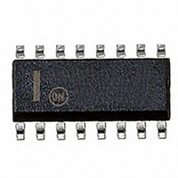
NCP1205DR2 ON Semiconductor, NCP1205DR2 Datasheet - Page 14

NCP1205DR2
Manufacturer Part Number
NCP1205DR2
Description
IC CTRLR PWM CM OVP HV 16SOIC
Manufacturer
ON Semiconductor
Datasheet
1.NCP1205DR2.pdf
(17 pages)
Specifications of NCP1205DR2
Output Isolation
Isolated
Frequency Range
90 ~ 125kHz
Voltage - Input
8 ~ 30 V
Operating Temperature
-25°C ~ 150°C
Package / Case
16-SOIC (0.154", 3.90mm Width)
Lead Free Status / RoHS Status
Contains lead / RoHS non-compliant
Other names
NCP1205DR2OS
Available stocks
Company
Part Number
Manufacturer
Quantity
Price
Part Number:
NCP1205DR2G
Manufacturer:
ON/安森美
Quantity:
20 000
back within its regulation area, the IC operation comes back
to normal.
8 x 128 ms delay is combined with the previous 128 ms. It
works as follows: the 128 ms delay is provided to account for
any normal transients that engender a temporary loss of
feedback (FB goes toward ground). However, when the
128 ms period is actually over (the feedback is definitively
lost) the IC stops the output driving pulses for a typical
period of 8 x 128 ms. During this mode, the rest of the
functions are still activated. For instance, in lack of pulses,
the self- -supplied being no longer provided, the startup
source turns on and off (when reaching the corresponding
UVLO
on the Vcc line. As soon as the feedback condition is
restored, the 8 x 128 ms is interrupted and, in synchronism
with the Vcc line, the IC is back to normal. The following
diagrams show how this mechanism takes place when FB is
down to zero (optocoupler opened) or up to Vcc
(optocoupler shorted). If we assume that the error is
permanently present, then a burst mode takes place with a
128/8 x 128 = 12.5% duty- -cycle. The real transmitted
power is thus:
As soon as the system recovers from the error, e.g. FB is
To avoid any system thermal runaway, another internal
Pout BURST = 1
L
and UVLO
H
2
levels), creating an hiccup waveform
· Lp · Ip 2 · Fsw · Duty BURST
http://onsemi.com
14
Overvoltage Detection (OVP)
allows to shutdown the controller as soon as the level on this
pin exceeds 2.8V, as detailed in Figure 16. In lack of
switching pulses, the Vcc capacitor is no longer refreshed by
the auxiliary supply and slowly discharges toward ground.
When the Vcc level crosses UVLOL, a new startup sequence
occurs. If the OVP has gone, the converter resumes its
operation.
Protecting Pin 1 Against Negative Spikes
negative voltages that could appear on it’s pins. To avoid any
adverse latch- -up of the IC, we strongly recommend
inserting a 15 k resistor in series with pin 1 and the
high- -voltage rail, as shown in Figures 17 and 18. This 15 k
resistor prevents from adversely latching the controller in
case of negative spikes appearing on the bulk capacitor
during the power- -off sequence. Please note that this resistor
does not dissipate any continuous power and can therefore
be of low power type. Two 8.2 k can also be wired in series
to sustain the large DC voltage present on the bulk.
Latched
OVP
Figure 16. In the PDIP- -8 Version, the OVP Pad is not
On the PDIP- -14 and the SOIC- -16 versions, an OVP pin
As any CMOS controller, NCP1205 is sensitive to
Pinned Out and is Available with PDIP- -14 Devices
2
+
--
7
1
Only
+
2.8 V
18 k
2 k
8
OVP


