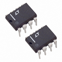
LT1512CN8#PBF Linear Technology, LT1512CN8#PBF Datasheet - Page 4

LT1512CN8#PBF
Manufacturer Part Number
LT1512CN8#PBF
Description
IC BATT CHRGR CONST I/V 8-DIP
Manufacturer
Linear Technology
Datasheet
1.LT1512CN8PBF.pdf
(12 pages)
Specifications of LT1512CN8#PBF
Function
Charge Management
Battery Type
All Battery Types
Voltage - Supply
2.7 V ~ 25 V
Operating Temperature
0°C ~ 70°C
Mounting Type
Through Hole
Package / Case
8-DIP (0.300", 7.62mm)
Lead Free Status / RoHS Status
Lead free / RoHS Compliant
Available stocks
Company
Part Number
Manufacturer
Quantity
Price
LT1512
TYPICAL PERFORMANCE CHARACTERISTICS
PIN FUNCTIONS
V
compensation, but it can also be used for soft starting and
current limiting. It is the output of the error amplifi er and
the input of the current comparator. Peak switch current
increases from 0A to 1.8A as the V
1V to 1.9V. Current out of the V
the pin is externally clamped below the internal 1.9V clamp
level. Loop frequency compensation is performed with a
capacitor or series RC network from the V
the ground pin (avoid ground loops).
4
C
: The compensation pin is primarily used for frequency
1.0
0.9
0.8
0.7
0.4
0.3
0.2
0.1
1.5
0.6
0.5
3.0
2.5
2.0
1.0
0.5
0
0
–50
0
Switch Saturation Voltage
vs Switch Current
Minimum Peak-to-Peak
Synchronization Voltage vs Temp
f
SYNC
0.2
–25
0.4
= 700kHz
0
SWITCH CURRENT (A)
0.6
TEMPERATURE (°C)
25
0.8
50
1.0
100°C
1.2
75
–55°C
150°C
1.4
100
1.6
C
125
25°C
pin is about 200μA when
1.8
1512 G01
1512 G04
150
2.0
C
voltage varies from
C
800
700
600
500
400
300
200
100
3.0
2.5
2.0
1.5
1.0
0.5
pin directly to
0
0
–50
0
Switch Current Limit
vs Duty Cycle
Feedback Input Current
vs Temperature
V
10
–25
FB
= V
20
REF
0
30
TEMPERATURE (°C)
DUTY CYCLE (%)
25
40
50
50
FB: The feedback pin is used for positive output voltage
sensing. This pin is the inverting input to the voltage
error amplifi er. The R1/R2 voltage divider connected to
FB defi nes Li-Ion fl oat voltage at full charge, or acts as a
voltage limiter for NiCd or NiMH applications. Input bias
current is typically 300nA, so divider current is normally
set to 100μA to swamp out any output voltage errors due
to bias current. The noninverting input of this amplifi er is
tied internally to a 1.245V reference. The grounded end of
the output voltage divider should be connected directly to
the LT1512 ground pin (avoid ground loops).
60
–55°C
75
70
100
25°C AND
125°C
80
125
90
1512 G02
1512 G05
100
150
–20
–10
–30
–40
–50
3.0
2.8
2.6
2.4
2.0
1.8
2.2
0
–50
–50
Minimum Input Voltage
vs Temperature
Negative Feedback Input Current
vs Temperature
–25
–25
0
0
TEMPERATURE (°C)
TEMPERATURE (°C)
25
25
50
50
75
75
100 125 150
100
125
1512 G06
1512 G03
1512fa
150


