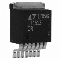
LT1513CR#PBF Linear Technology, LT1513CR#PBF Datasheet - Page 6

LT1513CR#PBF
Manufacturer Part Number
LT1513CR#PBF
Description
IC BATT CHRGR CONST/PROG I/V 7DD
Manufacturer
Linear Technology
Datasheet
1.LT1513-2CR.pdf
(16 pages)
Specifications of LT1513CR#PBF
Function
Charge Management
Battery Type
All Battery Types
Voltage - Supply
2.7 V ~ 25 V
Operating Temperature
0°C ~ 125°C
Mounting Type
Surface Mount
Package / Case
TO-263-8, D²Pak (7 leads + Tab), TO-263CA
Lead Free Status / RoHS Status
Lead free / RoHS Compliant
Available stocks
Company
Part Number
Manufacturer
Quantity
Price
OPERATION
LT1513/LT1513-2
BLOCK
The LT1513 is a current mode switcher. This means that
switch duty cycle is directly controlled by switch current
rather than by output voltage or current. Referring to the
Block Diagram, the switch is turned “on” at the start of each
oscillator cycle. It is turned “off” when switch current
reaches a predetermined level. Control of output voltage
and current is obtained by using the output of a dual
feedback voltage sensing error amplifier to set switch
current trip level. This technique has the advantage of
simplified loop frequency compensation. A low dropout
internal regulator provides a 2.3V supply for all internal
circuitry on the LT1513. This low dropout design allows
input voltage to vary from 2.7V to 25V. A 500kHz oscillator
is the basic clock for all internal timing. It turns “on” the
output switch via the logic and driver circuitry. Special
adaptive antisat circuitry detects onset of saturation in the
power switch and adjusts driver current instantaneously to
limit switch saturation. This minimizes driver dissipation
and provides very rapid turn-off of the switch.
A unique error amplifier design has two inverting inputs
which allow for sensing both output voltage and current. A
6
DIAGRAM
V
I
FB
FB
U
1.245V
REF
4k
50k*
S/S
W
*REMOVE ON LT1513-2
–
–
–
+
+
DELAY AND RESET
SYNC
I
FBA
EA
SHUTDOWN
500kHz
OSC
LOW DROPOUT
V
Figure 2
2.3V REG
C
COMP
LOGIC
V
IN
1.245V bandgap reference biases the noninverting input.
The first inverting input of the error amplifier is brought out
for positive output voltage sensing. The second inverting
input is driven by a “current” amplifier which is sensing
output current via an external current sense resistor. The
current amplifier is set to a fixed gain of – 12.5 which
provides a – 100mV current limit sense voltage.
The LT1513-2 option removes the feedback resistors
around the I
signal. This provides a ground referenced current sense
voltage suitable for external current programming and
makes amplifier input and output available for external
loop compensation.
The error signal developed at the amplifier output is
brought out externally and is used for frequency compen-
sation. During normal regulator operation this pin sits at a
voltage between 1V (low output current) and 1.9V (high
output current). Switch duty cycle goes to zero if the V
is pulled below the V
an idle mode.
A
V
6
IA
FB
+
–
amplifier and connects its output to the FB
DRIVER
C
pin threshold, placing the LT1513 in
ANTISAT
SW
LT1513 • BD
SWITCH
0.04
sn1513 1513fas
C
pin


