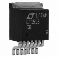
LT1513CR#PBF Linear Technology, LT1513CR#PBF Datasheet - Page 9

LT1513CR#PBF
Manufacturer Part Number
LT1513CR#PBF
Description
IC BATT CHRGR CONST/PROG I/V 7DD
Manufacturer
Linear Technology
Datasheet
1.LT1513-2CR.pdf
(16 pages)
Specifications of LT1513CR#PBF
Function
Charge Management
Battery Type
All Battery Types
Voltage - Supply
2.7 V ~ 25 V
Operating Temperature
0°C ~ 125°C
Mounting Type
Surface Mount
Package / Case
TO-263-8, D²Pak (7 leads + Tab), TO-263CA
Lead Free Status / RoHS Status
Lead free / RoHS Compliant
Available stocks
Company
Part Number
Manufacturer
Quantity
Price
APPLICATIONS
current Schottky diodes have relatively high leakage cur-
rents (5 A to 500 A) even at room temperature. The latest
very-low-forward devices have especially high leakage cur-
rents. It has been noted that surface mount versions of some
Schottky diodes have as much as ten times the leakage of
their through-hole counterparts. This may be because a low
forward voltage process is used to reduce power dissipation
in the surface mount package. In any case, check leakage
specifications carefully before making a final choice for the
switching diode. Be aware that diode manufacturers want
to specify a maximum leakage current that is ten times
higher than the typical leakage. It is very difficult to get them
to specify a low leakage current in high volume production.
This is an on going problem for all battery charger circuits
and most customers have to settle for a diode whose typical
leakage is adequate, but theoretically has a worst-case
condition of higher than desired battery drain.
Thermal Considerations
Care should be taken to ensure that worst-case conditions
do not cause excessive die temperatures. Typical thermal
resistance is 30 C/W for the R package but this number will
U
Figure 4. LT1513 Suggested Partial Layout for Critical Thermal and Electrical Paths
INFORMATION
U
C1,C3,C5 AND R3
TIED DIRECTLY TO
GROUND PLANE
C5
W
R5
LT1513 TAB AND GROUND
PIN SOLDERED TO
GROUND PLANE
GROUND PLANE
U
R3
C3
+
vary depending on the mounting technique (copper area,
airflow, etc.).
Average supply current (including driver current) is:
Switch power dissipation is given by:
Total power dissipation of the die is equal to supply current
times supply voltage, plus switch power:
For V
R
P
I
P
P
C1
L1A
I
P
+
IN
IN
SW
D(TOTAL)
SW
D
SW
IN
= 4mA + 24mA = 28mA
= (10)(0.028) + 0.64 = 0.92W
V
2 WINDING
= 10V, V
= 0.64W
INDUCTOR
IN
= Output switch ON resistance
4
C2
mA
V
(
C1
I
BAT
+
CHRG
= (I
BAT
IN
(
L1B
V
) (
)(V
2
BAT
= 8.2V, I
R
IN
D1
SW
) + P
)(
LT1513 • F04
I
CHRG
(
)(
V
V
IN
IN
V
SW
LT1513/LT1513-2
CHRG
BAT
)
2
)( .
0 024
= 1.2A, R
V
IN
)
)(
V
BAT
SW
= 0.3 ,
)
sn1513 1513fas
9


