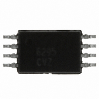
ISL6295CVZ Intersil, ISL6295CVZ Datasheet - Page 13

ISL6295CVZ
Manufacturer Part Number
ISL6295CVZ
Description
IC FUEL GAUGE LOW VOLTAGE8-TSSOP
Manufacturer
Intersil
Datasheet
1.ISL6295CVZ.pdf
(25 pages)
Specifications of ISL6295CVZ
Function
Fuel, Gas Gauge/Monitor
Battery Type
Lithium-Ion (Li-Ion), Lithium-Polymer (Li-Pol)
Voltage - Supply
2.8 V ~ 7 V
Operating Temperature
-20°C ~ 85°C
Mounting Type
Surface Mount
Package / Case
8-TSSOP
Battery Management Function
Fuel Gauge
Supply Voltage Range
2.8V To 7V
Interface Type
2-Wire, Serial, I2C
Battery Ic Case Style
TSSOP
No. Of Pins
8
Rohs Compliant
Yes
Lead Free Status / RoHS Status
Lead free / RoHS Compliant
Available stocks
Company
Part Number
Manufacturer
Quantity
Price
Company:
Part Number:
ISL6295CVZ
Manufacturer:
Intersil
Quantity:
40
Company:
Part Number:
ISL6295CVZ
Manufacturer:
INTERSIL
Quantity:
17
Part Number:
ISL6295CVZ
Manufacturer:
INTERSIL
Quantity:
20 000
Memory/Operational Register Description
Memory/Register Map
The ISL6295 internal structure is accessible on a strict
memory mapped basis. The only action directly taken by the
ISL6295 in response to an SMBus command is to read or
write registers, SRAM, or EEPROM locations. Any actions
taken by ISL6295 happen as a result of values written to
internal control registers.
Addressing in ISL6295 consists of 10 bits plus two bank
select bits. Therefore, there are a total of 4K byte locations
that are addressable within the ISL6295, organized as 4
banks of 1024 locations each. Bank 0 is dedicated for the
EEPROM. Bank 1 contains the general-purpose SRAM and
the data, status and control registers. Bank 2 contains test
registers, and Bank 3 is reserved.
PEC
Legend:
S
P
RS
A
A
BT
Bank
AH
Address low
S
RS
7
(Additional data bytes if BT =1)
7
7
7
13
SMBus Address
- Start
- Stop
- Repeated start
- Acknowdedge
- Negative Acknowledge (terminates transaction)
- Block mode indicator bit
- Controls selection of bank:
- Packet Error Code
- High order address bits (2)
- Low order address bits (8)
PEC (optional
Address Low
7
SMBus Address
00: EEPROM
01: RAM / Registers
FIGURE 8. ISL6295 SMBus READ TRANSACTION
)
1
0
0
0
0
0
A
A
A
1
ISL6295
1
0
10: Test Mode Registers
11: Reserved
A
P
7
BT
7
7
# of Bytes (only if BT = 1)
Table 1 describes the ISL6295 memory map. The notation is
y:0xzzz where y is the bank number and zzz is the register
address in HEX.
EEPROM
The 256 byte EEPROM is located in bank 0 and occupies
address 0:0x000 to 0:0x0FF. The EEPROM can be read
using Byte or Block transfer modes, but can only be written a
byte at a time. Writing the EEPROM takes approximately
4ms/byte. An EEPROM write cycle command from the
SMBus is immediately acknowledged by the ISL6295 if no
other EEPROM write cycles are in progress. If an EEPROM
read or write cycle is attempted while a previous request to
write is in progress, a negative Acknowledge will be returned
until the previous write cycle is completed.
A read or write to a register or SRAM location will not be
affected by an EEPROM write cycle in progress.
6
Last Read Data Byte
X
4
Bank
3
2
Master controls SDA
ISL6295 controls SDA
1
AH
0
0
0
A/A
A
A
February 8, 2011
FN9074.2


