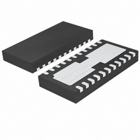
LTC4089EDJC-5#PBF Linear Technology, LTC4089EDJC-5#PBF Datasheet - Page 21

LTC4089EDJC-5#PBF
Manufacturer Part Number
LTC4089EDJC-5#PBF
Description
IC USB POWER MANAGER 22-DFN
Manufacturer
Linear Technology
Type
Battery Chargerr
Datasheet
1.LTC4089EDJCPBF.pdf
(24 pages)
Specifications of LTC4089EDJC-5#PBF
Function
Power Management
Battery Type
Lithium-Ion (Li-Ion)
Voltage - Supply
4.35 V ~ 5.5 V
Operating Temperature
-40°C ~ 85°C
Mounting Type
Surface Mount
Package / Case
22-WFDFN Exposed Pad
Output Voltage
4.2V
Operating Supply Voltage (min)
6V
Operating Supply Voltage (max)
36V
Operating Temp Range
-40C to 85C
Mounting
Surface Mount
Pin Count
22
Operating Temperature Classification
Industrial
Lead Free Status / RoHS Status
Lead free / RoHS Compliant
Available stocks
Company
Part Number
Manufacturer
Quantity
Price
APPLICATIONS INFORMATION
The power dissipation in the other power compo-
nents—catch diodes, MOSFETs, boost diodes and induc-
tors—causes additional copper heating and can further
increase the “ambient” temperature of the IC.
Board Layout Considerations
As discussed in the previous section, it is critical that
the exposed metal pad on the backside of the LTC4089/
LTC4089-5 package be soldered to the PC board ground.
Furthermore, proper operation and minimum EMI requires
a careful printed circuit board (PCB) layout. Note that large,
switched currents fl ow in the power switch (between the
HVIN and SW pins), the catch diode and the HVIN input
capacitor. These components, along with the inductor and
output capacitor, should be placed on the same side of
the circuit board, and their connections should be made
on that layer. Place a local, unbroken ground plane below
these components. The loop formed by these components
should be as small as possible. Additionally, the SW and
BOOST nodes should be kept as small as possible. Figure 8
shows the recommended component placement with trace
and via locations.
WITH C3 GND PAD
AND SEPERATED
VIAS CONNECTED TO ALL
SIDE-BY-SIDE
GND PLANES WITHOUT
C1 AND D1
GND PADS
SOLDERED TO PCB.
U1 THERMAL PAD
THERMAL RELIEF .
Figure 8. Suggested Board Layout
MINIMIZE TRACE LENGTH
MINIMIZE D1, L1,
C3, U1, SW PIN LOOP
V
Many types of capacitors can be used for input bypassing,
however, caution must be exercised when using multilayer
ceramic capacitors. Because of the self-resonant and high
Q characteristics of some types of ceramic capacitors,
high voltage transients can be generated under some
start-up conditions, such as from connecting the charger
input to a hot power source. For more information, refer
to Application Note 88.
Battery Charger Stability Considerations
The constant-voltage mode feedback loop is stable without
any compensation when a battery is connected with low
impedance leads. Excessive lead length, however, may add
enough series inductance to require a bypass capacitor
of at least 1μF from BAT to GND. Furthermore, a 4.7μF
capacitor with a 0.2 to 1 series resistor to GND is
recommended at the BAT pin to keep ripple voltage low
when the battery is disconnected.
High frequency currents, such as the high voltage input
current of the LTC4089, tend to fi nd their way along
the ground plane on a mirror path directly beneath the
incident path on the top of the board. If there are slits or
cuts in the ground plane due to other traces on that layer,
the current will be forced to go around the slits. If high
frequency currents are not allowed to fl ow back through
their natural least-area path, excessive voltage will build
up and radiated emissions will occur. See Figure 9.
IN
and V
Figure 9. Ground Currents Follow Their Incident Path
at High Speed. Slices in the Ground Plane Cause High
Voltage and Increased Emissions.
HVIN
Bypass Capacitor
LTC4089/LTC4089-5
4089 F09
21
40895fc


