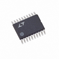
LTC4011CFE#TR Linear Technology, LTC4011CFE#TR Datasheet - Page 18

LTC4011CFE#TR
Manufacturer Part Number
LTC4011CFE#TR
Description
IC BATT CHARGER HIEFF 20TSSOP
Manufacturer
Linear Technology
Datasheet
1.LTC4011CFEPBF.pdf
(26 pages)
Specifications of LTC4011CFE#TR
Function
Charge Management
Battery Type
Nickel Cadmium (NiCd), Nickel Metal-Hydride (NiMH)
Voltage - Supply
4.5 V ~ 34 V
Operating Temperature
0°C ~ 85°C
Mounting Type
Surface Mount
Package / Case
20-TSSOP (0.173", 4.40mm Width) Exposed Pad
Lead Free Status / RoHS Status
Contains lead / RoHS non-compliant
Available stocks
Company
Part Number
Manufacturer
Quantity
Price
LTC4011
applicaTions inForMaTion
operations. However, this practice is not recommended
for NiMH cells charged well above or below their 1C rate,
because fast charge termination based solely on voltage
inflection may not be adequate to protect the battery from
a severe overcharge. A resistor between 10k and 20k may
be used to connect V
still desired.
INTV
If BGATE is left open, the INTV
be used as an additional source of regulated voltage in the
host system any time READY is active. Switching loads
on INTV
circuits used to monitor and terminate fast charging.
In addition, DC current drawn from the INTV
greatly increase internal power dissipation at elevated V
voltages. A minimum ceramic bypass capacitor of 0.1µF
is recommended.
Calculating Average Power Dissipation
The user should ensure that the maximum rated IC junction
temperature is not exceeded under all operating conditions.
The thermal resistance of the LTC4011 package (θ
is 38°C/W, provided the exposed metal pad is properly
soldered to the PCB. The actual thermal resistance in the
application will depend on the amount of PCB copper to
which the package is soldered. Feedthrough vias directly
below the package that connect to inner copper layers
are helpful in lowering thermal resistance. The following
formula may be used to estimate the maximum average
power dissipation P
normal operating conditions.
where:
I
I
Q
network from V
in coulombs
DD
VRT
TGATE
DD
= Average external INTV
= Load current drawn by the external thermistor
Regulator Output
DD
= Gate charge of external P-channel MOSFET
may reduce the accuracy of internal analog
RT
, if any
D
TEMP
(in watts) of the LTC4011 under
to V
DD
RT
DD
if the pause function is
pin of the LTC4011 can
load current, if any
DD
pin can
JA
CC
)
Q
V
R
n = Number of LEDs driven by the LTC4011
Sample Applications
Figures 6 through 9 detail sample charger applications
of various complexities. Combined with the Typical Ap-
plication on the first page of this data sheet, these Figures
demonstrate some of the proper configurations of the
LTC4011. MOSFET body diodes are shown in these figures
strictly for reference only.
Figure 6 shows a minimum application, which might be
encountered in low cost NiCd fast charge applications.
FET-based PowerPath control allows for maximum input
voltage range from the DC adapter. The LTC4011 uses
–∆V to terminate the fast charge state, as no external
temperature information is available. Nonsynchronous
PWM switching is employed to reduce external component
cost. A single LED indicates charging status.
A 3A NiMH application of medium complexity is shown in
Figure 7. PowerPath control that is completely FET-based
allows for both minimum input voltage overhead and mini-
mum switchover loss when operating from the battery.
P-channel MOSFET Q4 functions as a switch to connect the
battery to the system load whenever the DC input adapter
is removed. If the maximum battery voltage is less than
the maximum rated V
are not required. Otherwise choose the Zener voltage
of D1 to be less than the maximum rated V
provides a bias current of (V
D1 when the input adapter is removed. Choose R5 to make
this current, which is drawn from the battery, just large
enough to develop the desired V
Precharge, fast charge and top-off states are indicated by
external LEDs. The V
LTC4011 to accurately terminate fast charge under a variety
of applied charge rates. Use of a synchronous PWM topol-
ogy improves efficiency and lowers power dissipation.
(if used) in coulombs
the application
LED
BGATE
LED
= Maximum external LED forward voltage
= External LED current-limiting resistor used in
= Gate charge of external N-channel MOSFET
TEMP
GS
of Q4, diode D1 and resistor R5
thermistor network allows the
BAT
– V
GS
across D1.
ZENER
)/(R5 + 20k) for
GS
of Q4. R5
4011fb


