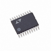
LTC4011CFE#TR Linear Technology, LTC4011CFE#TR Datasheet - Page 23

LTC4011CFE#TR
Manufacturer Part Number
LTC4011CFE#TR
Description
IC BATT CHARGER HIEFF 20TSSOP
Manufacturer
Linear Technology
Datasheet
1.LTC4011CFEPBF.pdf
(26 pages)
Specifications of LTC4011CFE#TR
Function
Charge Management
Battery Type
Nickel Cadmium (NiCd), Nickel Metal-Hydride (NiMH)
Voltage - Supply
4.5 V ~ 34 V
Operating Temperature
0°C ~ 85°C
Mounting Type
Surface Mount
Package / Case
20-TSSOP (0.173", 4.40mm Width) Exposed Pad
Lead Free Status / RoHS Status
Contains lead / RoHS non-compliant
Available stocks
Company
Part Number
Manufacturer
Quantity
Price
applicaTions inForMaTion
2. Place the LTC4011 close to the switching FET gate
3. Place the inductor input as close as possible to the
4. Place the charge current sense resistor immediately
5. Place output capacitors adjacent to the sense resisitor
6. Output capacitor ground connections must feed into
capacitors. Vias should not be used to make these
connections.
terminals, keeping the connecting traces short to
produce clean drive signals. This rule also applies to IC
supply and ground pins that connect to the switching
FET source pins. The IC can be placed on the opposite
side of the PCB from the switching FETs.
drain of the switching FETs. Minimize the surface area
of the switch node. Make the trace width the minimum
needed to support the programmed charge current.
Use no copper fills or pours. Avoid running the con-
nection on multiple copper layers in parallel. Minimize
capacitance from the switch node to any other trace
or plane.
adjacent to the inductor output, and orient it such that
current sense traces to the LTC4011 are short. These
feedback traces need to be run together as a single pair
with the smallest spacing possible on any given layer
on which they are routed. Locate any filter component
on these traces next to the LTC4011, and not at the
sense resistor location.
output and ground.
the same copper that connects to the input capacitor
ground before tying back into system ground.
V
IN
C
Figure 13. High Speed Switching Path
IN
SWITCHING GROUND
CIRCULATING
FREQUENCY
SWITCH NODE
HIGH
PATH
L1
D1
C
OUT
4011 F13
BAT
V
BAT
7. Connection of switching ground to system ground,
8. Route analog ground as a trace tied back to the LTC4011
9. A good rule of thumb for via count in a given high
10. If possible, place all the parts listed above on the same
11. Copper fills or pours are good for all power connec-
12. For best current programming accuracy, provide a
13. It is important to minimize parasitic capacitance on the
or any internal ground plane should be single-point.
point to make the connection.
GND pin before connecting to any other ground. Avoid
using the system ground plane. A useful CAD technique
is to make analog ground a separate ground net and
use a 0Ω resistor to connect analog ground to system
on multiple layers can also be used in parallel. This
these pins to their respective resistors should be as
short as possible.
If the system has an internal system ground plane, a
good way to do this is to cluster vias into a single star
ground.
current path is to use 0.5A per via. Be consistent when
applying this rule.
PCB layer.
tions except as noted above in Rule 3. Copper planes
helps with thermal management and lowers trace in-
ductance, which further improves EMI performance.
Kelvin connection from R
See Figure 14 for an example.
TIMER, SENSE and BAT pins. The traces connecting
Figure 14. Kelvin Sensing of Charge Current
DIRECTION OF CHARGING CURRENT
SENSE
R
SENSE
SENSE
BAT
to SENSE and BAT.
4011 F14
LTC4011
4011fb


