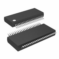
LTC6802IG-1#PBF Linear Technology, LTC6802IG-1#PBF Datasheet - Page 9

LTC6802IG-1#PBF
Manufacturer Part Number
LTC6802IG-1#PBF
Description
IC MONITOR BATT STACK MC 44-SSOP
Manufacturer
Linear Technology
Datasheet
1.LTC6802IG-1PBF.pdf
(38 pages)
Specifications of LTC6802IG-1#PBF
Function
Battery Monitor
Battery Type
Lithium-Ion (Li-Ion)
Voltage - Supply
4 V ~ 50 V
Operating Temperature
-40°C ~ 85°C
Mounting Type
Surface Mount
Package / Case
44-SOP (0.200", 5.30mm Width)
Lead Free Status / RoHS Status
Lead free / RoHS Compliant
Available stocks
Company
Part Number
Manufacturer
Quantity
Price
PIN FUNCTIONS
GPIO1, GPIO2 (Pins 38, 39): General Purpose Input/Out-
put. The operation of these pins depends on the state of
the MMB pin.
When MMB is high, the pins behave as traditional GPIOs.
By writing a “0” to a GPIO configuration register bit, the
open drain output is activated and the pin is pulled to V
By writing a logic “1” to the configuration register bit, the
corresponding GPIO pin is high impedance. An external
resistor is needed to pull the pin up to V
By reading the configuration register locations GPIO1
and GPIO2, the state of the pins can be determined. For
example, if a “0” is written to register bit GPIO1, a “0” is
always read back because the output NMOSFET pulls pin
38 to V
becomes high impedance. Either a “1” or a “0” is read
back, depending on the voltage present at pin 38. The
GPIOs makes it possible to turn on/off circuitry around
the LTC6802-1, or read logic values from a circuit around
the LTC6802-1.
When the MMB pin is low, the GPIO pins and the WDTB
pin are treated as inputs that set the number of cells to
be monitored. See Monitor Mode in the Applications
Information section.
V
V
voltage inputs and outputs. This means these pins accept
MODE
REG
, the SCKI, SDI, SDO, and CSBI pins are configured as
(Pin 40): Voltage Mode Input. When V
–
. If a “1” is written to register bit GPIO1, the pin
REG
MODE
.
is tied to
–
.
standard TTL logic levels. Connect V
the LTC6802-1 is the bottom device in a daisy chain.
When V
pins are configured as current inputs and outputs, and SDO
is unused. Connect V
being driven by another LTC6802-1 in a daisy chain.
SCKI (Pin 41): Serial Clock Input. The SCKI pin interfaces
to any logic gate (TTL levels) if V
must be driven by the SCKO pin of another LTC6802-1 if
V
Information section.
SDI (Pin 42): Serial Data Input. The SDI pin interfaces to
any logic gate (TTL levels) if V
must be driven by the SDOI pin of another LTC6802-1 if
V
Information section.
SDO (Pin 43): Serial Data Output. The SDO pin is an NMOS
open drain output if V
if V
Information section.
CSBI (Pin 44): Chip Select (Active Low) Input. The CSBI
pin interfaces to any logic gate (TTL levels) if V
to V
LTC6802-1 if V
Applications Information section.
MODE
MODE
MODE
REG
is tied to V
is tied to V
. CSBI must be driven by the CSBO pin of another
MODE
is tied to V
is connected to V
MODE
–
–
. See Serial Port in the Applications
. See Serial Port in the Applications
–
MODE
. See Serial Port in the Applications
is tied to V
MODE
is tied to V
to V
–
MODE
MODE
, the SCKI, SDI, and CSBI
–
–
when the LTC6802-1 is
. See Serial Port in the
LTC6802-1
REG
MODE
is tied to V
is tied to V
. SDO is not used
to V
MODE
REG
REG
REG
. SCKI
is tied
when
. SDI
68021fa
9


