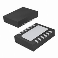
ISL9212IRZ Intersil, ISL9212IRZ Datasheet - Page 9

ISL9212IRZ
Manufacturer Part Number
ISL9212IRZ
Description
IC SAFETY SYSTEM CHARGER 12-TDFN
Manufacturer
Intersil
Datasheet
1.ISL9212IRZ-T.pdf
(11 pages)
Specifications of ISL9212IRZ
Function
Battery Monitor
Battery Type
Lithium-Ion (Li-Ion)
Voltage - Supply
4.3 V ~ 6.5 V
Operating Temperature
-40°C ~ 85°C
Mounting Type
Surface Mount
Package / Case
12-TDFN
Battery Protection
Over Voltage
No. Of Batteries
1
Supply Voltage Range
4.3V To 6.5V
Battery Ic Case Style
TDFN
No. Of Pins
12
Operating Temperature Range
-40°C To +85°C
Rohs Compliant
Yes
Lead Free Status / RoHS Status
Lead free / RoHS Compliant
Available stocks
Company
Part Number
Manufacturer
Quantity
Price
Company:
Part Number:
ISL9212IRZ
Manufacturer:
Intersil
Quantity:
256
Company:
Part Number:
ISL9212IRZ-T
Manufacturer:
INTERSIL
Quantity:
2 322
Part Number:
ISL9212IRZ-T
Manufacturer:
INTERSIL
Quantity:
20 000
R
The R
battery terminal, in case the ISL9212 fails. The
recommended value should be between 200kΩ to 1MΩ.
With 200kΩ resistance, the worst case current flowing from
the VB pin to the charger output is:
assuming the VB pin voltage is 30V under a failure mode
and the battery voltage is 4.2V. Such a small current can be
easily absorbed by the bias current of other components in
the handheld system. Increasing the R
worst case current, but at the same time increases the error
for the 4.4V battery OVP threshold.
The error of the battery OVP threshold is the original
accuracy at the VB pin given in the “Electrical Specifications”
table on page 2 plus the voltage built across the R
VB pin leakage current. The VB pin leakage current is less
than 20nA, as given in the “Electrical Specifications” table.
With the 200kΩ resistor, the worst-case additional error is
4mV and with a 1MΩ resistor, the worst-case additional error
is 20mV.
Interfacing to MCU
The ISL9212 has the enable (EN) and the warning (WRN)
digital signals that can be interfaced to a microcontroller unit
(MCU). Both signals can be left floating if not used. When
interfacing to an MCU, it is highly recommended to insert a
resistor between the ISL9212 signal pin and the MCU GPIO
pin, as shown in Figure 24. The resistor creates an isolation
to limit the current, in case a high voltage shows up at the
ISL9212 pins under a failure mode. The recommended
resistance ranges from 10kΩ to 100kΩ. The selection of the
R
should be selected so that the ISL9212 EN pin voltage is
above the disable threshold when the GPIO output of the
MCU is high.
(
30V
1000
EN
VB
is dependent on the IO voltage (VIO) of the MCU. R
–
Selection
0
VB
FIGURE 23. LITHIUM-SAFE OPERATING REGIONS
4.2V )
prevents a large current from the VB pin to the
⁄
(
200kΩ
1
ISL9212
LIMITS
ISL6292C
LIMITS
=
130μA
2
BATTERY VOLTAGE (V)
)
9
3
VB
4
value reduces the
5
VB
(EQ. 2)
by the
EN
6
ISL9212
Capacitor Selection
The input capacitor (C
page 1) is for decoupling. Higher value reduces the voltage
drop or the over shoot during transients.
Two scenarios can cause the input voltage over shoot. The
first one is when the AC adapter is inserted live (hot insertion)
and the second one is when the current in the power PFET of
the ISL9212 has a step-down change. Figure 25 shows an
equivalent circuit for the ISL9212 input. The cable between the
AC/DC converter output and the handheld system input has a
parasitic inductor. The parasitic resistor is the lumped sum of
various components, such as the cable, the adapter output
capacitor ESR, the connector contact resistance, and so on.
During the load current step-down transient, the energy
stored in the parasitic inductor is used to charge the input
decoupling capacitor C
the power PFET slowly during the OCP, the battery OVP
event, and when the device is disabled via the EN pin.
Because of such design, the input over shoot during those
events is not significant. During an input OVP, however, the
PFET is turned in less than 1µs and can lead to significant
over shoot. Higher capacitance reduces this type of over
shoot.
The over shoot caused by a hot insertion is not very
dependent on the decoupling capacitance value. Especially
when ceramic type capacitors are used for decoupling. In
theory, the over shoot can rise up to twice of the DC output
voltage of the AC adapter. The actual peak voltage is
FIGURE 25. EQUIVALENT CIRCUIT FOR THE ISL9212 INPUT
ISL9212
AC/DC
FIGURE 24. DIGITAL SIGNAL INTERFACE BETWEEN ISL9212
Q
ADAPTER
5
C1
Q
4
AND MCU
R
5
L
1
WRN
EN
2
CABLE
in the “Typical Application Circuit” on
. The ISL9212 is designed to turn off
R
R
PU
R
R
WRN
EN
VIO
C2
HANDHELD SYSTEM
June 30, 2008
ISL9212
MCU
FN9280.2


