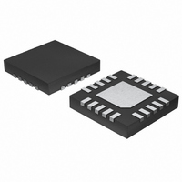
MAX17006BETP+ Maxim Integrated Products, MAX17006BETP+ Datasheet - Page 12

MAX17006BETP+
Manufacturer Part Number
MAX17006BETP+
Description
IC BATT CHARGER 1.2MHZ 20-TQFN
Manufacturer
Maxim Integrated Products
Specifications of MAX17006BETP+
Function
Charge Management
Battery Type
Multi-Chemistry
Voltage - Supply
8 V ~ 26 V
Operating Temperature
-40°C ~ 85°C
Mounting Type
Surface Mount
Package / Case
20-TQFN Exposed Pad
Lead Free Status / RoHS Status
Lead free / RoHS Compliant
1.2MHz, Low-Cost,
High-Performance Chargers
The VCTL input adjusts the battery-output voltage,
V
4-cell applications, use the MAX17005B; for 2- and
3-cell applications, use the MAX17006B. Use the
MAX17015B to adjust the cell number and set the cell
voltage with a resistive voltage-divider from the output.
Based on the version of the part, the number of cells
and the level of VCTL should be set as in Table 1.
The MAX17005B/MAX17006B support from 4.2V/cell to
4.4V/cell, whereas the MAX17015B supports minimum
2.1V. The maximum voltage is determined with the
dropout performance of IC. When the required voltage
falls outside the range available with the MAX17005B or
MAX17006B, the MAX17015B should be used.
The charge-voltage regulation for the MAX17005B and
MAX17006B is calculated with the following equations:
for 3-cell selection of MAX17005B and MAX17006B,
4.2V > VCTL > 2.4V:
for 2- or 4-cell selection of MAX17006B or MAX17005B,
respectively, 0 < VCTL < 1.8V. Connect VCTL to GND
or to V
For the MAX17015B, connect VCTL to GND to set the FB
regulation point to 2.1V. The charge-voltage regulation is
calculated with the following equation:
12
Table 1. Cell Configuration
MAX17005B
MAX17005B
MAX17006B
MAX17006B
MAX17015B
BATT
VERSION
______________________________________________________________________________________
, and determines the number of cells. For 3- and
AA
for default 4.2V/cell battery-voltage setting.
V
CHG REG
NO. OF CELLS
V
_
CELL
Sets FB
V
CELL
3
4
2
3
=
=
V
V
=
FB SETPOINT
AA
Setting Charge Voltage
V
_
AA
+
V
VCTL = AGND or VCTL = V
+
AA
V
VCTL
2.4V < VCTL < 4.2V
2.4V < VCTL < 4.2V
-
6
6
0 < VCTL < 1.8V
0 < VCTL < 1.8V
V
VCTL
×
R
LEVEL
8
R
+
8
R
7
AA
Figure 3. MAX17015B Charge-Voltage Regulation Feedback
Network
There are two constraints in choosing R7 and R8. The
resistors cannot be too small since they discharge the
battery, and they cannot be too large because FB pin
consumes less than 1µA of input bias current. Pick R8
to be approximately 10kΩ and then calculate R7.
FB regulation error (±0.5% max) and the tolerance of R7
and R8 both contribute to the error on the battery volt-
age. Use 0.1% feedback resistors for best accuracy.
Figure 3 shows the MAX17015B charge-voltage regula-
tion feedback network.
The voltage at ISET determines the voltage across cur-
rent-sense resistor RS2. ISET can accept either analog
or digital inputs. The full-scale differential voltage
between CSIP and CSIN is 80mV (8A for RS2 = 10mΩ)
for the analog input, and 60mV (6A for RS2 = 10mΩ) for
the digital PWM input.
When the MAX17005B/MAX17006B/MAX17015B power
up and the charger is ready, if there is no clock edge
within 20ms, the circuit assumes ISET is an analog
input, and disables the PWM filter block. To configure
the charge current, force the voltage on ISET according
to the following equation:
The input range for ISET is from 0 to V
down the charger, pull ISET below 26mV.
If there is a clock edge on ISET within 20ms, the PWM
filter is enabled and ISET accepts digital PWM input.
The PWM filter has a DAC with 8-bit resolution that cor-
responds to equivalent V
MAX17015B
CSIN
FB
I
CHG
=
240
CSIP-CSIN
RS
Setting Charge Current
mV
2
C
OUT
×
V
V
ISET
AA
steps.
R7
R8
AA
/2. To shut
BATTERY


