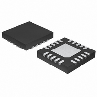
MAX17006BETP+ Maxim Integrated Products, MAX17006BETP+ Datasheet - Page 9

MAX17006BETP+
Manufacturer Part Number
MAX17006BETP+
Description
IC BATT CHARGER 1.2MHZ 20-TQFN
Manufacturer
Maxim Integrated Products
Specifications of MAX17006BETP+
Function
Charge Management
Battery Type
Multi-Chemistry
Voltage - Supply
8 V ~ 26 V
Operating Temperature
-40°C ~ 85°C
Mounting Type
Surface Mount
Package / Case
20-TQFN Exposed Pad
Lead Free Status / RoHS Status
Lead free / RoHS Compliant
Dual Mode is a trademark of Maxim Integrated Products, Inc.
PIN
10
11
12
13
14
15
16
17
18
19
20
—
1
2
3
4
5
6
7
8
9
BATT/FB
NAME
AGND
PGND
CSSN
CSSP
DCIN
ACIN
VCTL
CSIN
CSIP
ISET
DLO
LDO
IINP
BST
DHI
V
CC
BP
_______________________________________________________________________________________
LX
AA
Charger Bias Supply Input. Bypass DCIN with a 1µF capacitor to PGND.
Analog Ground
Output Current-Sense Positive Input. Connect a current-sense resistor from CSIP to CSIN.
Output Current-Sense Negative Input
Input Current-Monitor Output. IINP sources the current proportional to the current sensed across
CSSP and CSSN. The transconductance from (CSSP - CSSN) to IINP is 2.8µA/mV. See the Analog
Input Current-Monitor Output section to configure the current monitor for a particular gain setting.
Battery Voltage Feedback Input. For the MAX17015B, connect a resistor voltage-divider from the
battery output to FB (see Figure 1).
AC Detect Output. This open-drain output is high impedance when ACIN is lower than V
Connect a 10k
Input Current Sense for Positive Input. Connect a current-sense resistor from CSSP to CSSN.
Input Current-Sense Negative Input
Dual Mode™ Input for Setting Maximum Charge Current. ISET can be configured either with a
resistor voltage-divider or with a PWM signal from 128Hz to 500kHz. If there is no clock edge
within 20ms, ISET defaults to analog input mode. Pull ISET to AGND to shut down the charger. In
the MAX17015B, when the adapter is absent, drive ISET above 1V to enable IINP during battery
discharge. When the adapter is reinserted, ISET must be released to the correct control level within
300ms.
Power Ground Connection for MOSFET Drivers
Low-Side Power-MOSFET Driver Output. Connect to low-side n-channel MOSFET gate.
Linear-Regulator Output. LDO provides the power to the MOSFET drivers. LDO is the output of the 5.4V
linear regulator supplied from DCIN. Bypass LDO with a 4.7µF ceramic capacitor from LDO to PGND.
High-Side Driver Supply. Connect a 0.68µF capacitor from BST to LX.
High-Side Power-MOSFET Driver Output. Connect to high-side n-channel MOSFET gate.
High-Side Driver Source Connection. Connect a 0.68µF capacitor from BST to LX.
AC Adapter Detect Input. ACIN is the input to an uncommitted comparator.
4.2V Voltage Reference and Device Power-Supply Input. Bypass V
Voltage Regulation Loop-Compensation Point. Connect a 0.01µF capacitor from CC to AGND.
Battery Voltage Adjust Input. VCTL sets the number of cells and adjusts the voltage per cell. The
adjustment range is 4.2V to 4.4V per cell. See the Setting Charge Voltage section.
Backside Paddle. Connect the backside paddle to analog ground.
pullup resistor from LDO to
High-Performance Chargers
FUNCTION
1.2MHz, Low-Cost,
.
AA
with a 1µF capacitor to AGND.
Pin Description
AA
/2.
9


