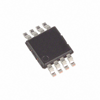
DS2740U+ Maxim Integrated Products, DS2740U+ Datasheet - Page 5

DS2740U+
Manufacturer Part Number
DS2740U+
Description
IC CURRENT GAUGE(15BIT) 8UMAX
Manufacturer
Maxim Integrated Products
Datasheet
1.DS2740BU.pdf
(16 pages)
Specifications of DS2740U+
Function
Current Gauge (15 Bit)
Voltage - Input
2.7 ~ 5.5 V
Operating Temperature
-40°C ~ 85°C
Mounting Type
Surface Mount
Package / Case
8-MSOP, Micro8™, 8-uMAX, 8-uSOP,
Battery Type
Li-Ion, NiMH
Operating Supply Voltage
2.7 V to 5.5 V
Maximum Operating Temperature
+ 85 C
Minimum Operating Temperature
- 40 C
Charge Safety Timers
No
Mounting Style
SMD/SMT
Temperature Monitoring
No
Lead Free Status / RoHS Status
Lead free / RoHS Compliant
Current - Output
-
Accuracy
-
Sensing Method
-
Lead Free Status / Rohs Status
Lead free / RoHS Compliant
POWER MODES
The DS2740 has two power modes: Active and Sleep. While in Active mode, the DS2740 operates as a
high-precision coulomb counter with current and accumulated current measurement blocks operating
continuously and the resulting values updated in the measurement registers. Read and write access is
allowed to all registers. PIO pin is active. In Sleep mode, the DS2740 operates in a low-power mode with
no current measurement activity. Serial access to current, accumulated current, and status/control
registers is allowed if V
The DS2740 operating mode transitions from SLEEP to ACTIVE when:
The DS2740 operating mode transitions from ACTIVE to SLEEP when:
CURRENT MEASUREMENT
In the Active mode of operation, the DS2740 continually measures the current flow into and out of the
battery by measuring the voltage drop across a low-value current-sense resistor, R
range for pulse-type load currents, the voltage signal can be filtered by adding a capacitor between the
IS1 and IS2 pins. The external capacitor and two internal resistors form a lowpass filter at the input of the
ADC. The voltage-sense range at IS1 and IS2 is ±51.2mV. The input converts peak signal amplitudes up
to 102mV as long as the continuous or average signal level (post filter) does not exceed ±51.2mV over
the conversion cycle period. The ADC samples the input differentially at IS1 and IS2 with an 18.6kHz
sample clock and updates the current register at the completion of each conversion cycle. Conversion
times for each resolution option are listed in the tables below. Two resolution options are available.
Figure 3 describes the current measurement register format and resolution for each option. “S” indicates
the sign bit(s).
Figure 3. CURRENT REGISTER FORMAT
DS2740U : Units: 1.5625 μ V/R
DS2740BU : Units: 6.250 μ V/R
1)
2)
1)
2)
MSb
Full-scale magnitude: ±51.2mV
S
V
SMOD = 1 and DQ < V
DQ > V
2
V
14
DD
DD
MSB—Address 0Eh
falls to UV threshold, or
rises from below UV threshold to above UV threshold.
2
13
IH
DD
, and V
2
> 2V.
12
2
DD
11
SNS
SNS
> UV threshold, or
2
, 15-bit + sign resolution, 3.5s conversion period.
10
, 13-bit + sign resolution, 0.875s conversion period.
IL
for 2s.
2
9
LSb
2
8
5 of 16
MSb
2
7
2
6
LSB—Address 0Fh
2
5
2
4
2
3
SNS
2
. To extend the input
2
2
1
LSb
2
0


