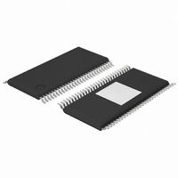
PCF8576CTT/1,118 NXP Semiconductors, PCF8576CTT/1,118 Datasheet - Page 29

PCF8576CTT/1,118
Manufacturer Part Number
PCF8576CTT/1,118
Description
IC LCD DVR UNIVERSAL 56-HTSSOP
Manufacturer
NXP Semiconductors
Datasheet
1.PCF8576CTT1118.pdf
(57 pages)
Specifications of PCF8576CTT/1,118
Package / Case
56-TSSOP Exposed Pad, 56-eTSSOP, 56-HTSSOP
Display Type
LCD
Configuration
40 Segment
Interface
I²C
Current - Supply
120µA
Voltage - Supply
2 V ~ 6 V
Operating Temperature
-40°C ~ 85°C
Mounting Type
Surface Mount
Number Of Digits
20
Number Of Segments
160
Maximum Clock Frequency
315 KHz
Operating Supply Voltage
2 V to 6 V
Maximum Power Dissipation
400 mW
Maximum Supply Current
120 uA
Lead Free Status / RoHS Status
Lead free / RoHS Compliant
Digits Or Characters
-
Lead Free Status / Rohs Status
Lead free / RoHS Compliant
Other names
935284868118
PCF8576CTT/1-T
PCF8576CTT/1-T
PCF8576CTT/1-T
PCF8576CTT/1-T
NXP Semiconductors
PCF8576C
Product data sheet
7.18.3 Device-select command
7.18.4 Bank-select command
7.18.5 Blink-select command
7.19 Display controller
Table 11.
Table 12.
[1]
Table 13.
[1]
[2]
The display controller executes the commands identified by the command decoder. It
contains the status registers of the PCF8576C and coordinates their effects. The
controller is also responsible for loading display data into the display RAM as required by
the filling order.
Bit
7
6 to 4
3 to 0
Bit
7
6 to 2
1
0
Bit
7
6 to 3
2
1 to 0
The bank-select command has no effect in 1:3 and 1:4 multiplex drive modes.
Normal blinking is assumed when the LCD multiplex drive modes 1:3 or 1:4 are selected.
Alternate RAM bank blinking does not apply in 1:3 and 1:4 multiplex drive modes.
Symbol
C
-
A[2:0]
Symbol
C
-
I
O
Symbol
C
-
AB
BF[1:0]
Device-select command bit description
Bank-select command bit description
Blink-select command bit description
All information provided in this document is subject to legal disclaimers.
0, 1
000 to 111
0, 1
Value
1100
Value
0, 1
11110
0
1
0
1
Value
1110
0
1
00
01
10
11
Rev. 10 — 22 July 2010
Description
see
fixed value
3 bit binary value, 0 to 7; transferred to the subaddress
counter to define one of eight hardware subaddresses
Description
see
fixed value
blink mode selection
blink frequency selection
Description
Static
see
fixed value
input bank selection; storage of arriving display data
output bank selection; retrieval of LCD display data
normal blinking
alternate RAM bank blinking
off
1
2
3
RAM bit 0
RAM bit 2
RAM bit 0
RAM bit 2
Figure 20
Figure 20
Figure 20
Universal LCD driver for low multiplex rates
[1]
[2]
1:2 multiplex
RAM bits 0 and 1
RAM bits 2 and 3
RAM bits 0 and 1
RAM bits 2 and 3
PCF8576C
© NXP B.V. 2010. All rights reserved.
[1]
29 of 57


