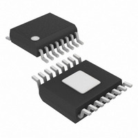
MAX6951CEE+T Maxim Integrated Products, MAX6951CEE+T Datasheet - Page 15

MAX6951CEE+T
Manufacturer Part Number
MAX6951CEE+T
Description
IC DRVR DSPL LED SRL 16-QSOP
Manufacturer
Maxim Integrated Products
Datasheet
1.MAX6950CEE.pdf
(19 pages)
Specifications of MAX6951CEE+T
Display Type
LED
Configuration
7 Segment
Interface
3-Wire Serial
Digits Or Characters
8 Digits
Current - Supply
10mA
Voltage - Supply
2.7 V ~ 5.5 V
Operating Temperature
0°C ~ 70°C
Mounting Type
Surface Mount
Package / Case
16-QSOP Exposed Pad, 16-eQSOP , 16-HQSOP
Number Of Digits
8
Number Of Segments
64
Low Level Output Current
400 mA
High Level Output Current
- 50 mA
Operating Supply Voltage
2.7 V to 5.5 V
Maximum Supply Current
15 mA
Maximum Power Dissipation
667 mW
Maximum Operating Temperature
+ 70 C
Mounting Style
SMD/SMT
Minimum Operating Temperature
0 C
Lead Free Status / RoHS Status
Lead free / RoHS Compliant
Table 16. No-Decode Mode Data Bits and
Corresponding Segment Lines
K
R
C
C
pF, typically 3pF
The recommended value of R
ommended value of C
The recommended value of R
allowed value, since it sets the display driver to the
maximum allowed segment current. R
a higher value to set the segment current to a lower
peak value where desired. The user must also ensure
that the peak current specifications of the LEDs con-
nected to the driver are not exceeded.
The effective value of C
external capacitor used, but also the stray capacitance
from the OSC pin to GND. This capacitance is usually
in the 1pF to 5pF range, depending on the layout used.
The display connection scheme used by the
MAX6950/MAX6951 puts LED segments in reverse bias
during a portion of the multiplexing time. The maximum
applied reverse bias voltage is the value of the supply
voltage, V+. It is therefore important to ensure that the
F
SET
SET
STRAY
Segment line
= 6720
= external resistor in kΩ
= external capacitor in pF
= stray capacitance from OSC pin to GND in
LED Maximum Reverse Voltage
D7
dp
______________________________________________________________________________________
f
e
D6
SET
a
SET
is 27pF.
D5
a
g
d
b
REGISTER DATA
includes not only the actual
SET
Serially Interfaced, +2.7V to +5.5V,
D4
c
SET
is 56kΩ and the rec-
5- and 8-Digit LED Display Drivers
b
c
D3
d
SET
is the minimum
D2
e
can be set to
d
D1
f
D0
g
LEDs chosen are rated to withstand a reverse bias
equal to the maximum supply voltage applied to the
MAX6950/MAX6951.
The MAX6950/MAX6951 drive a peak current of 40mA
into LEDs with a 2.4V forward-voltage drop when oper-
ated from a supply voltage of at least 3.0V. The mini-
mum voltage drop across the internal LED drivers is
therefore (3.0V - 2.4V) = 0.6V. If a higher supply volt-
age is used, the driver absorbs a higher voltage, and
the driver’s power dissipation increases accordingly.
However, if the LEDs used have a higher forward volt-
age drop than 2.4V, the supply voltage must be raised
accordingly to ensure that the driver always has at least
0.6V headroom.
The voltage drop across the drivers with a nominal +5V
supply (5.0V - 2.4V) = 2.6V is nearly 3 times the drop
across the drivers with a nominal 3.3V supply (3.3V -
2.4V) = 0.9V. In many systems, consumption is an
important design criterion, and the MAX6950/MAX6951
should be operated from the system’s 3.3V nominal
supply. In other designs, the lowest supply voltage may
be 5V. The issue now is to ensure the dissipation limit
for the MAX6950/MAX6951 is not exceeded. This can
be achieved by inserting a series resistor in the supply
to the MAX6950/MAX6951, ensuring that the supply
decoupling capacitors are still on the MAX6950/
MAX6951 side of the resistor. For example, consider
the requirement that the minimum supply voltage to a
MAX6951 must be 3.0V, and the input supply range is
5V ±5%. Maximum supply current is 15mA + (40mA
8) = 335mA. Minimum input supply voltage is 4.75V.
Maximum series resistor value is (4.75V - 3.0V)/0.335A
= 5.2Ω. We choose 4.7Ω ±10%. Worst-case resistor
dissipation is at maximum toleranced resistance, i.e.,
(0.335A)
resistor rating. The maximum MAX6951 supply voltage
is at maximum input supply voltage and minimum toler-
anced resistance, i.e., 5.25V - (0.335A
3.83V.
The MAX6950/MAX6951 work over the +2.7V to +5.5V
supply range. The minimum useful supply voltage is
determined by the forward voltage drop of the LEDs at
the peak current I
by the driver output stages. The MAX6950/MAX6951
correctly regulate I
mum voltage. If the supply drops below this minimum
voltage, the driver output stages may brown out, and
Choosing Supply Voltage to Minimize
2
✕
(4.7Ω
Applications Information
SEG
✕
SEG
1.1) = 0.584W. We choose a 1W
, plus the 0.6V headroom required
with a supply above this mini-
Low-Voltage Operation
Power Dissipation
✕
4.7Ω
✕
0.9) =
15
✕


