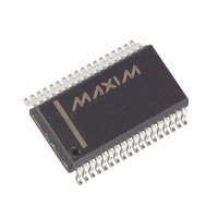
MAX6953EAX+T Maxim Integrated Products, MAX6953EAX+T Datasheet - Page 19

MAX6953EAX+T
Manufacturer Part Number
MAX6953EAX+T
Description
IC DRVR DSPL LED 36-SSOP
Manufacturer
Maxim Integrated Products
Datasheet
1.MAX6953EAX.pdf
(23 pages)
Specifications of MAX6953EAX+T
Display Type
LED
Configuration
5 x 7 (Matrix)
Interface
I²C
Digits Or Characters
4 Digits
Current - Supply
12mA
Voltage - Supply
2.7 V ~ 5.5 V
Operating Temperature
-40°C ~ 85°C
Mounting Type
Surface Mount
Package / Case
36-SSOP
Number Of Digits
4
Number Of Segments
140
Low Level Output Current
500 mA
High Level Output Current
50 mA
Operating Supply Voltage
2.7 V to 5.5 V
Maximum Supply Current
15 mA
Maximum Power Dissipation
941.2 mW
Maximum Operating Temperature
+ 85 C
Mounting Style
SMD/SMT
Minimum Operating Temperature
- 40 C
Lead Free Status / RoHS Status
Lead free / RoHS Compliant
4MHz, which makes the blink frequencies 0.5Hz selec-
table between 1Hz. The recommended value of R
also sets the peak current to 40mA, which makes the
segment current adjustable from 2.5mA to 37.5mA in
2.5mA steps:
where:
K
K
R
C
C
pF, typically 2pF
The recommended value of R
recommended value of C
The recommended value of R
allowed value since it sets the display driver to the
maximum allowed segment current. R
a higher value to set the segment current to a lower
peak value where desired. The user must also ensure
that the peak current specifications of the LEDs con-
nected to the driver are not exceeded.
The effective value of C
external capacitor used, but also the stray capacitance
from OSC to GND. This capacitance is usually in the
1pF to 5pF range, depending on the layout used.
The display-test register switches the drivers between
one of two modes: normal and display test. Display-test
mode turns all LEDs on by overriding, but not altering,
all control and digit registers (including the shutdown
register). In display-test mode, eight digits are scanned
and the duty cycle is 7/16 (half power). Table 22 lists
the display-test register format.
Table 22. Display-Test Register Format
Normal operation
Display test
I
F
SET
SET
STRAY
= 2144
= 6003
= external resistor in kΩ
= external capacitor in pF
I
f
SEG
OSC
MODE
= stray capacitance from OSC pin to GND in
2-Wire Interfaced, 2.7V to 5.5V, 4-Digit 5
= K
= K
I
F
/ R
/ (R
______________________________________________________________________________________
SET
SET
CODE (HEX)
ADDRESS
mA
SET
SET
0x07
0x07
(C
Display-Test Register
includes not only the actual
SET
is 26pF.
SET
+ C
SET
is 53.6kΩ and the
STRAY
SET
is the minimum
D7
X
X
can be set to
)) MHz
D6
X
X
SET
Matrix LED Display Driver
D5
X
X
The MAX6953 drives a peak current of 40mA into LEDs
with a 2.4V forward-voltage drop when operated from a
supply voltage of at least 3.0V. The minimum voltage
drop across the internal LED drivers is therefore (3.0V -
2.4V) = 0.6V. If a higher supply voltage is used, the dri-
ver absorbs a higher voltage, and the driver’s power
dissipation increases accordingly. However, if the LEDs
used have a higher forward voltage drop than 2.4V, the
supply voltage must be raised accordingly to ensure
that the driver always has at least 0.6V headroom.
The voltage drop across the drivers with a nominal 5V
supply (5.0V - 2.4V) = 2.6V is nearly 3 times the drop
across the drivers with a nominal 3.3V supply (3.3V -
2.4V) = 0.9V. In most systems, consumption is an
important design criterion, and the MAX6953 should be
operated from the system’s 3.3V nominal supply. In
other designs, the lowest supply voltage may be 5V.
The issue now is to ensure that the dissipation limit for
the MAX6953 is not exceeded. This can be achieved
by inserting a series resistor in the supply to the
MAX6953, ensuring that the supply decoupling capaci-
tors are still on the MAX6953 side of the resistor. For
example, consider the requirement that the minimum
supply voltage to a MAX6953 must be 3.0V, and the
input supply range is 5V ±5%. Maximum supply current
is:
Minimum input supply voltage is 4.75V. Maximum
series resistor value is:
We choose 3.3Ω ±5%. Worst-case resistor dissipation
is at maximum toleranced resistance, i.e., (0.415A)
(3.3Ω x 1.05) = 0.577W. We choose a 1W resistor rat-
ing. The maximum MAX6953 supply voltage is at maxi-
mum input supply voltage and minimum toleranced
resistance, i.e., 5.25V - (0.415A
REGISTER DATA
Choosing Supply Voltage to Minimize
D4
X
X
(4.75V - 3.0V) / 0.415A = 4.22Ω
15mA + (40mA
Applications Information
D3
X
X
D2
X
X
10) = 415mA
Power Dissipation
3.3Ω
D1
X
X
0.95) = 3.95V.
D0
0
1
2
7
19


