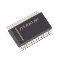
MAX6953EAX+T Maxim Integrated Products, MAX6953EAX+T Datasheet - Page 5

MAX6953EAX+T
Manufacturer Part Number
MAX6953EAX+T
Description
IC DRVR DSPL LED 36-SSOP
Manufacturer
Maxim Integrated Products
Datasheet
1.MAX6953EAX.pdf
(23 pages)
Specifications of MAX6953EAX+T
Display Type
LED
Configuration
5 x 7 (Matrix)
Interface
I²C
Digits Or Characters
4 Digits
Current - Supply
12mA
Voltage - Supply
2.7 V ~ 5.5 V
Operating Temperature
-40°C ~ 85°C
Mounting Type
Surface Mount
Package / Case
36-SSOP
Number Of Digits
4
Number Of Segments
140
Low Level Output Current
500 mA
High Level Output Current
50 mA
Operating Supply Voltage
2.7 V to 5.5 V
Maximum Supply Current
15 mA
Maximum Power Dissipation
941.2 mW
Maximum Operating Temperature
+ 85 C
Mounting Style
SMD/SMT
Minimum Operating Temperature
- 40 C
Lead Free Status / RoHS Status
Lead free / RoHS Compliant
(Typical application circuit, V+ = 3.3V, LED forward voltage = 2.4V, scan limit set to 4 digits, T
105
100
1, 2, 3, 6–14, 23, 24
95
90
85
80
25–31, 34, 35, 36
2.5
DEAD CLOCK OSCILLATOR FREQUENCY
4, 5, 17
SSOP
32, 33
2-Wire Interfaced, 2.7V to 5.5V, 4-Digit 5
15
16
18
19
20
21
22
3.0
—
vs. SUPPLY VOLTAGE
SUPPLY VOLTAGE (V)
3.5
_______________________________________________________________________________________
4.0
PIN
4.5
1, 2, 3, 7–15, 26, 27
28–34, 38, 39, 40
4, 5, 6, 19
35, 36, 37
5.0
16, 25
PDIP
17
18
20
21
22
23
24
5.5
1.01
1.00
0.99
0.98
0.97
0.96
0.95
Typical Operating Characteristics (continued)
2.5
O14 to O23
3.0
O0 to O13
OUTPUT SOURCE CURRENT
NAME
BLINK
vs. SUPPLY VOLTAGE
GND
ISET
N.C.
OSC
SDA
AD1
AD0
SCL
V+
SUPPLY VOLTAGE (V)
Matrix LED Display Driver
3.5
4.0
LED Cathode Drivers. O0 to O13 outputs sink current from
the display’s cathode rows.
Ground
Segment Current Setting. Connect ISET to GND through
series resistor R
Address Input 1. Sets device slave address. Connect to
either GND, V+, SCL, SDA to give four logic combinations.
See Table 3.
Not Connected
Blink Output. Output is open drain.
Multiplex Clock Input. To use internal oscillator, connect
capacitor C
drive OSC with a 1MHz to 8MHz CMOS clock.
Address Input 0. Sets device slave address. Connect to
either GND, V+, SCL, SDA to give four logic combinations.
See Table 3.
I
I
LED Anode Drivers. O14 to O23 outputs source current to
the display’s anode columns.
Positive Supply Voltage. Bypass V+ to GND with a 47µF
bulk capacitor and a 0.1µF ceramic capacitor.
2
2
4.5
C-Compatible Serial Data I/O
C-Compatible Serial Clock Input
5.0
SET
5.5
from OSC to GND. To use external clock,
GROUND FOR
GROUND FOR
SET
CATHODE
(PIN 014)
(PIN 03)
to set the peak current.
ANODE
A
= +25°C, unless otherwise noted.)
FUNCTION
WAVEFORMS AT O2 (PIN 3) AND O14
(PIN 28) V+ = 3.3V, 8/16 INTENSITY
Pin Description
200µs/div
7
5


