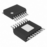
MAX6951CEE+ Maxim Integrated Products, MAX6951CEE+ Datasheet - Page 11

MAX6951CEE+
Manufacturer Part Number
MAX6951CEE+
Description
IC DRVR DSPL LED SRL 16-QSOP
Manufacturer
Maxim Integrated Products
Datasheet
1.MAX6950CEE.pdf
(19 pages)
Specifications of MAX6951CEE+
Display Type
LED
Configuration
7 Segment
Interface
3-Wire Serial
Digits Or Characters
8 Digits
Current - Supply
10mA
Voltage - Supply
2.7 V ~ 5.5 V
Operating Temperature
0°C ~ 70°C
Mounting Type
Surface Mount
Package / Case
16-QSOP Exposed Pad, 16-eQSOP , 16-HQSOP
Number Of Digits
8
Number Of Segments
64
Low Level Output Current
400000 uA
High Level Output Current
- 50000 uA
Operating Supply Voltage
2.7 V to 5.5 V
Maximum Supply Current
15000 uA
Maximum Power Dissipation
667 mW
Maximum Operating Temperature
+ 70 C
Mounting Style
SMD/SMT
Minimum Operating Temperature
0 C
Lead Free Status / RoHS Status
Lead free / RoHS Compliant
If the blink function is disabled through the Blink Enable
Bit E (Table 8) in the configuration register, then the digit
register data in plane P0 is used to multiplex the display.
The digit register data in P1 is not used (Table 17).
If the blink function is enabled, then the digit register
data in both plane P0 and plane P1 are alternately used
to multiplex the display. Blinking is achieved by multi-
plexing the LED display using data plane P0 and plane
P1 on alternate phases of the blink clock (Table 18).
The display blinking facility, when enabled, makes the
driver flip automatically between displaying the digit
register data in planes P0 and plane P1. If the digit reg-
ister data for any individual segment is different in the
two planes, then that segment appears to blink or flash
Table 10. Global Clear Digit Data (R Data Bit D5) Format
Table 12. Scan-Limit Register Format
Table 11. Display-Test Register Format
Digit data for both
planes P0 and P1 are
unaffected
Digit data for both
planes P0 and P1 are
cleared on the rising
edge of CS
Normal operation
Display test
Display digit 0 only
Display digits 0 and 1
Display digits 0 and 1 2
Display digits 0 and 1 2 3
Display digits 0 and 1 2 3 4
Display digits 0 and 1 2 3 4 5
Display digits 0 and 1 2 3 4 5 6
Display digits 0 and 1 2 3 4 5 6 7
MODE
MODE
SCAN LIMIT
______________________________________________________________________________________
CODE (HEX)
CODE (HEX)
ADDRESS
ADDRESS
0x04
0x04
0x07
0x07
Display Blink Mode
Serially Interfaced, +2.7V to +5.5V,
5- and 8-Digit LED Display Drivers
CODE (HEX)
ADDRESS
0x03
0x03
0x03
0x03
0x03
0x03
0x03
0x03
D7
D7
X
X
X
X
D7
X
X
X
X
X
X
X
X
D6
D6
X
X
X
X
D6
X
X
X
X
X
X
X
X
on and off. Once blinking has been configured, it con-
tinues automatically without further intervention.
The blink speed is determined by frequency of the mul-
tiplex clock, OSC, and by the setting of the Blink Rate
Selection Bit B (Table 7) in the configuration register.
The Blink Rate Selection Bit B sets either fast or slow
blink speed for the whole display.
The OSC input pin is used to set both the display scan
rate and the blink timing for the display driver. OSC
must either be fitted with an external capacitor C
GND to set the frequency of the MAX6950/MAX6951s’
internal RC oscillator, or be overdriven with an external
TTL/CMOS clock.
D5
D5
X
X
0
1
D5
X
X
X
X
X
X
X
X
REGISTER DATA
REGISTER DATA
REGISTER DATA
Multiplex Clock and OSC Oscillator
D4
D4
T
T
X
X
D4
X
X
X
X
X
X
X
X
D3
D3
D3
X
X
X
X
X
X
X
X
E
E
X
X
D2
0
0
0
0
1
1
1
1
D2
D2
B
B
X
X
D1
0
0
1
1
0
0
1
1
D1
D1
Blink Speed
0
0
X
X
D0
0
1
0
1
0
1
0
1
CODE
SET
D0
D0
0xX0
0xX1
0xX2
0xX3
0xX4
0xX5
0xX6
0xX7
HEX
S
S
0
1
11
to


