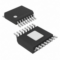
MAX6951CEE+ Maxim Integrated Products, MAX6951CEE+ Datasheet - Page 7

MAX6951CEE+
Manufacturer Part Number
MAX6951CEE+
Description
IC DRVR DSPL LED SRL 16-QSOP
Manufacturer
Maxim Integrated Products
Datasheet
1.MAX6950CEE.pdf
(19 pages)
Specifications of MAX6951CEE+
Display Type
LED
Configuration
7 Segment
Interface
3-Wire Serial
Digits Or Characters
8 Digits
Current - Supply
10mA
Voltage - Supply
2.7 V ~ 5.5 V
Operating Temperature
0°C ~ 70°C
Mounting Type
Surface Mount
Package / Case
16-QSOP Exposed Pad, 16-eQSOP , 16-HQSOP
Number Of Digits
8
Number Of Segments
64
Low Level Output Current
400000 uA
High Level Output Current
- 50000 uA
Operating Supply Voltage
2.7 V to 5.5 V
Maximum Supply Current
15000 uA
Maximum Power Dissipation
667 mW
Maximum Operating Temperature
+ 70 C
Mounting Style
SMD/SMT
Minimum Operating Temperature
0 C
Lead Free Status / RoHS Status
Lead free / RoHS Compliant
Figure 1. Timing Diagram
Figure 2. Transmission of 16 Bits to the MAX6950/MAX6951
Figure 3 . Transmission of More than 16 Bits to the MAX6950/MAX6951
control registers remains unaltered. Shutdown can be
used to save power. For minimum supply current in
shutdown mode, logic inputs should be at ground or
V+ (CMOS-logic levels). The display driver can be pro-
grammed while in shutdown mode, and shutdown
mode can be overridden by the display test function.
Table 7 lists the blink rate selection format.
If blink is globally enabled by setting the E bit of the
configuration register (Table 8), then the digit data in
both planes P0 and P1 are used to control the display
(Table 9).
CLK
DIN
CLK
CS
DIN
CS
BIT1
CLK
DIN
CS
BIT2
D15
_______________________________________________________________________________________
D14
N-15
D13
N-14
D12
Serially Interfaced, +2.7V to +5.5V,
N-13
5- and 8-Digit LED Display Drivers
t
CSS
t
DS
D11
N-12
D15
t
DH
D10
N-11
t
CL
N-10
D14
D9
t
CH
N-9
D8
N-8
When the global blink timing synchronization bit is set,
the multiplex and blink timing counter is cleared on the
rising edge of CS. By setting the T bit in multiple
MAX6950/MAX6951s at the same time (or in quick suc-
cession), the blink timing can be synchronized across
all the devices.
When the global digit data clear (R data bit D5) is set,
the digit data for both planes P0 and P1 for ALL digits
is cleared on the rising edge of CS. Digits with decode
enabled display the zero. Digits without decode
enabled show all segments unlit.
D7
D1
N-7
D6
t
CP
N-6
D5
D0
N-5
t
CSH
D4
N-4
t
D3
CSW
N-3
D2
N-2
D1
N-1
D0
N
7


