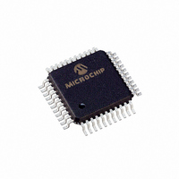
TC835CKW Microchip Technology, TC835CKW Datasheet - Page 11

TC835CKW
Manufacturer Part Number
TC835CKW
Description
IC ADC 4 1/2DGT BCD 44-MQFP
Manufacturer
Microchip Technology
Datasheet
1.TC835CKW.pdf
(26 pages)
Specifications of TC835CKW
Display Type
LED
Configuration
7 Segment
Interface
BCD
Digits Or Characters
A/D 4.5 Digits
Current - Supply
1mA
Voltage - Supply
4 V ~ 6 V
Operating Temperature
0°C ~ 70°C
Mounting Type
Surface Mount
Package / Case
44-MQFP, 44-PQFP
Lead Free Status / RoHS Status
Lead free / RoHS Compliant
Available stocks
Company
Part Number
Manufacturer
Quantity
Price
Company:
Part Number:
TC835CKW
Manufacturer:
Microchip Technology
Quantity:
10 000
Part Number:
TC835CKW
Manufacturer:
MICROCHIP/微芯
Quantity:
20 000
Company:
Part Number:
TC835CKW713
Manufacturer:
Microchip Technology
Quantity:
10 000
5.4
If the input signal causes the reference voltage integra-
tion time to exceed 20,000 clock pulses, the
OVERRANGE output is set to a logic "1." The
overrange output register is set when BUSY goes low,
and is reset at the beginning of the next reference
integration phase.
5.5
If the output count is 9% of full scale or less (-1800
counts), the underrange register bit is set at the end of
BUSY. The bit is set low at the next signal integration
phase.
5.6
A positive input is registered by a logic "1" polarity
signal. The POLARITY bit is valid at the beginning of
Reference Integrate and remains valid until determined
during the next conversion.
The POLARITY bit is valid even for a zero reading.
Signals less than the converter's LSB will have the
signal polarity determined correctly. This is useful in
null applications.
© 2007 Microchip Technology Inc.
OVERRANGE Output
UNDERRANGE Output
POLARITY Output
5.7
Digit drive signals are positive going signals. The scan
sequence is D
pulses wide, except D
All five digits are scanned continuously, unless an over-
range condition occurs. In an overrange condition, all
digit drives are held low from the final STROBE pulse
until the beginning of the next reference integrate
phase. The scanning sequence is then repeated. This
provides a blinking visual display indication.
5.8
The binary coded decimal (BCD) bits B
positive-true logic signals. The data bits become active
simultaneously with the digit drive signals. In an
overrange condition, all data bits are at a logic "0" state.
Digit Drive Outputs
BCD Data Outputs
5
to D
1
. All positive pulses are 200 clock
5
, which is 201 clock pulses wide.
DS21478C-page 11
TC835
8
, B
4
, B
2
, B
1
are


