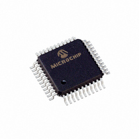
TC835CKW Microchip Technology, TC835CKW Datasheet - Page 7

TC835CKW
Manufacturer Part Number
TC835CKW
Description
IC ADC 4 1/2DGT BCD 44-MQFP
Manufacturer
Microchip Technology
Datasheet
1.TC835CKW.pdf
(26 pages)
Specifications of TC835CKW
Display Type
LED
Configuration
7 Segment
Interface
BCD
Digits Or Characters
A/D 4.5 Digits
Current - Supply
1mA
Voltage - Supply
4 V ~ 6 V
Operating Temperature
0°C ~ 70°C
Mounting Type
Surface Mount
Package / Case
44-MQFP, 44-PQFP
Lead Free Status / RoHS Status
Lead free / RoHS Compliant
Available stocks
Company
Part Number
Manufacturer
Quantity
Price
Company:
Part Number:
TC835CKW
Manufacturer:
Microchip Technology
Quantity:
10 000
Part Number:
TC835CKW
Manufacturer:
MICROCHIP/微芯
Quantity:
20 000
Company:
Part Number:
TC835CKW713
Manufacturer:
Microchip Technology
Quantity:
10 000
FIGURE 3-2:
3.2.2
The TC835 integrates the differential voltage between
the +INPUT and -INPUT pins. The differential voltage
must be within the device Common mode range (-1V
from either supply rail, typically). The input signal polar-
ity is determined at the end of this phase (see
Figure
FIGURE 3-3:
Phase.
3.2.3
The previously charged reference capacitor is con-
nected with the proper polarity to ramp the integrator
output back to zero (see
ing displayed is:
TABLE 3-6:
© 2007 Microchip Technology Inc.
Analog
Common
Analog
Common
Conversion Cycle Phase
System Zero
Input Signal Integration
Reference Voltage Integration
Integrator Output Zero
*Note:
REF
+IN
+IN
REF
IN
IN
IN
IN
SW
SW
SW
SW
3-3).
SW
SW
SW
SW
Z
Z
R
Reading = 10,000
R
I
I
I
I
Assumes a positive polarity input signal. SW
ANALOG INPUT SIGNAL
INTEGRATION
REFERENCE VOLTAGE
INTEGRATION
C
C
REF
REF
INTERNAL ANALOG GATE STATUS
SW
SW
Input Buffer
Input Buffer
1
1
Analog
Analog
SW
SW
+
-
System Zero Phase.
+
–
Input Signal Integration
SW
SW
IZ
IZ
Figure
Z
Z
[Differential Input]
SW
SW
R
R
INT
INT
Z
Z
3-4). The digital read-
Integrator
Integrator
Closed
V
SW
C
C
REF
C
C
—
—
—
+
-
+
–
SZ
SZ
INT
Switch Open
Switch Closed
INT
Switch Open
Switch Closed
I
Closed*
+
–
+
-
SW
Comparator
Comparator
—
—
—
RI
+
To
Digital
Section
To
Digital
Section
RI
SW
would be closed for a negative input signal.
—
—
—
—
RI
-
Closed
SW
—
—
—
FIGURE 3-4:
Integration Cycle.
3.2.4
This phase guarantees the integrator output is at 0V
when the system zero phase is entered and that the
true system offset voltages are compensated for. This
phase normally lasts 100 to 200 clock cycles. If an
overrange condition exists, the phase is extended to
6200 clock cycles (see
FIGURE 3-5:
Phase.
Analog
Common
Analog
Common
Z
REF
REF
+IN
+IN
IN
IN
IN
IN
SW
SW
SW
SW
SW
Closed
SW
SW
SW
SW
Z
Z
—
—
—
R
R
I
I
I
I
R
INTEGRATOR OUTPUT ZERO
C
C
REF
REF
Closed
Closed
Closed
SW
SW
SW
—
Input Buffer
Input Buffer
1
1
1
Analog
SW
Analog
SW
+
–
Reference Voltage
Integrator Output Zero
+
SW
–
SW
Figure
IZ
IZ
Z
Closed
Z
SW
SW
—
—
—
SW
R
R
IZ
3-5).
INT
Z
INT
Z
Integrator
Integrator
C
C
C
C
Reference Figures
+
–
+
SZ
–
SZ
INT
INT
Switch Open
Switch Closed
Switch Open
Switch Closed
DS21478C-page 7
TC835
Figure 3-2
Figure 3-3
Figure 3-4
Figure 3-5
+
–
+
–
Comparator
Comparator
To
Digital
Section
To
Digital
Section


