CS5463-ISZ Cirrus Logic Inc, CS5463-ISZ Datasheet - Page 27
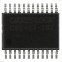
CS5463-ISZ
Manufacturer Part Number
CS5463-ISZ
Description
IC ENERGY METERING 1PHASE 24SSOP
Manufacturer
Cirrus Logic Inc
Datasheet
1.CS5463-ISZ.pdf
(46 pages)
Specifications of CS5463-ISZ
Package / Case
24-SSOP
Input Impedance
30 KOhm
Measurement Error
0.1%
Voltage - I/o High
0.8V
Voltage - I/o Low
0.2V
Current - Supply
2.9mA
Voltage - Supply
4.75 V ~ 5.25 V
Operating Temperature
-40°C ~ 85°C
Mounting Type
Surface Mount
Meter Type
Single Phase
Output Voltage Range
2.4 V to 2.6 V
Input Voltage Range
2.4 V to 2.6 V
Input Current
25 nA
Power Dissipation
500 mW
Operating Temperature Range
- 40 C to + 85 C
Mounting Style
SMD/SMT
Input Voltage
5.25V
No. Of Outputs
3
Power Dissipation Pd
500mW
Supply Voltage Range
3.3V To 5V
No. Of Pins
24
Filter Terminals
SMD
Supply Voltage Min
3.3V
Rohs Compliant
Yes
Frequency
20GHz
Lead Free Status / RoHS Status
Lead free / RoHS Compliant
For Use With
598-1553 - BOARD EVAL & SOFTWARE CS5463 ADC
Lead Free Status / Rohs Status
Lead free / RoHS Compliant
Other names
598-1096-5
Available stocks
Company
Part Number
Manufacturer
Quantity
Price
Company:

Part Number:
CS5463-ISZ
Manufacturer:
CIRRUS
Quantity:
39
Company:
Part Number:
CS5463-ISZ
Manufacturer:
CS
Quantity:
1 045
Part Number:
CS5463-ISZ
Manufacturer:
CIRRUS
Quantity:
20 000
Company:
Part Number:
CS5463-ISZR
Manufacturer:
CYPRESS
Quantity:
1 001
Part Number:
CS5463-ISZR
Manufacturer:
CIRRUS
Quantity:
20 000


6.1.2 Current and Voltage DC Offset Register ( I
6.1.3 Current and Voltage Gain Register ( I
6.1.4 Cycle Count Register ( Cycle Count )
6.1.5 PulseRateE Register ( PulseRateE )
DS678F2
MSB
MSB
MSB
MSB
-(2
-(2
2
2
23
1
Address: 1 (Current DC Offset); 3 (Voltage DC Offset)
0
Default = 0x000000
The DC Offset registers (I
register is updated with the DC offset measured over a computation cycle. DRDY will be set at the end of the
calibration. This register may be read and stored for future system offset compensation. The value is represent-
ed in two's complement notation and in the range of -1.0 ≤ I
the MSB. See Section 7.1.2.1
Address: 2 (Current Gain); 4 (Voltage Gain)
Default = 0x400000 = 1.000
The gain registers (I
the register is updated with the gain measured over a computation cycle. DRDY will be set at the end of the
calibration. This register may be read and stored for future system gain compensation. The value is in the range
0.0 ≤ I
0
Address: 5
Default = 0x000FA0 = 4000
Cycle Count, denoted as N, determines the length of one computation cycle . During continuous conversions,
the computation cycle frequency is (MCLK/K)/(1024 ∗ N). A one second computational cycle period occurs when
MCLK = 4.096 MHz, K = 1, and N = 4000.
Address: 6
Default = 0x800000 = 1.00 (2 kHz @ 4.096 MHz MCLK)
PulseRateE sets the frequency of E1, E2, & E3 pulses. E1, E2, E3 frequency = (MCLK x PulseRateE) / 2048 at
full scale. For a 4 khz sample rate, the maximum pulse rate is 2 khz. The value is represented in two's comple-
ment notation and in the range is -1.0 ≤ PulseRateE < 1.0, with the binary point to the right of the MSB. Negative
values have the same effect as positive. See Section 5.5
)
)
2
2
2
2
gn
22
-1
-1
0
,V
gn
2
2
2
2
< 3.9999, with the binary point to the right of the second MSB.
21
-2
-1
-2
2
2
2
2
gn
20
-3
-2
-3
,V
gn
DCoff
)
2
2
2
are initialized to 1.0 on reset. When either a AC or DC Gain calibration is performed,
2
19
-4
-3
-4
,V
DC Offset Calibration Sequence
DCoff
2
2
2
2
18
-5
-4
-5
)
are initialized to 0.0 on reset. When DC Offset calibration is performed, the
2
2
2
2
17
-6
-5
-6
gn
2
2
2
2
16
-7
-6
-7
, V
DCoff
gn
.....
.....
.....
.....
)
Energy Pulse Output
, V
DCoff
DCoff
2
2
2
, V
2
-17
-16
-17
on page 37 for more information.
6
DCoff
)
2
2
2
2
< 1.0, with the binary point to the right of
-18
-17
-18
5
2
2
2
2
-19
-18
-19
on page 17 for more information.
4
2
2
2
2
-20
-19
-20
3
2
2
2
2
-21
-20
-21
2
CS5463
2
2
2
2
-22
-21
-22
1
LSB
LSB
LSB
LSB
2
2
2
2
-23
-22
-23
0
27
Related parts for CS5463-ISZ
Image
Part Number
Description
Manufacturer
Datasheet
Request
R

Part Number:
Description:
Single Phase, Bidirectional Power/Energy
Manufacturer:
Cirrus Logic Inc
Datasheet:

Part Number:
Description:
Other Power Management Single Phase Power/Energy IC
Manufacturer:
Cirrus Logic Inc
Datasheet:

Part Number:
Description:
RF COILS < SMD Type: CS Series>
Manufacturer:
SUMIDA [Sumida Corporation]
Datasheet:

Part Number:
Description:
Development Kit
Manufacturer:
Cirrus Logic Inc
Datasheet:
Part Number:
Description:
Development Kit
Manufacturer:
Cirrus Logic Inc
Datasheet:


Part Number:
Description:
High-efficiency PFC + Fluorescent Lamp Driver Reference Design
Manufacturer:
Cirrus Logic Inc
Datasheet:
Part Number:
Description:
Development Kit
Manufacturer:
Cirrus Logic Inc
Datasheet:
Part Number:
Description:
Development Kit
Manufacturer:
Cirrus Logic Inc
Datasheet:

Part Number:
Description:
Development Kit
Manufacturer:
Cirrus Logic Inc
Datasheet:
Part Number:
Description:
Development Kit
Manufacturer:
Cirrus Logic Inc
Datasheet:
Part Number:
Description:
Development Kit
Manufacturer:
Cirrus Logic Inc
Datasheet:
Part Number:
Description:
Development Kit
Manufacturer:
Cirrus Logic Inc
Datasheet:

Part Number:
Description:
Ref Bd For Speakerbar MSA & DSP Products
Manufacturer:
Cirrus Logic Inc