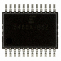
CS5460A-BSZ Cirrus Logic Inc, CS5460A-BSZ Datasheet - Page 38

CS5460A-BSZ
Manufacturer Part Number
CS5460A-BSZ
Description
IC ENERGY METERING 1PHASE 24SSOP
Manufacturer
Cirrus Logic Inc
Datasheet
1.CS5460A-BSZ.pdf
(54 pages)
Specifications of CS5460A-BSZ
Package / Case
24-SSOP
Input Impedance
30 KOhm
Measurement Error
0.1%
Voltage - I/o High
0.8V
Voltage - I/o Low
0.2V
Current - Supply
2.9mA
Voltage - Supply
4.75 V ~ 5.25 V
Operating Temperature
-40°C ~ 85°C
Mounting Type
Surface Mount
Meter Type
Single Phase
Output Voltage Range
2.4 V to 2.6 V
Output Current
1 uA
Input Voltage Range
2.4 V to 2.6 V
Input Current
25 nA
Power Dissipation
500 mW
Operating Temperature Range
- 40 C to + 85 C
Mounting Style
SMD/SMT
Ic Function
Single Phase Bi-directional Power / Energy IC
Brief Features
On-Chip Functions, AC Or DC System Calibration, Power Supply Monitor
Supply Voltage Range
3.3V To 5V
Rohs Compliant
Yes
Lead Free Status / RoHS Status
Lead free / RoHS Compliant
For Use With
CDB5460AU - EVALUATION BOARD FOR CS5460A
Lead Free Status / Rohs Status
Lead free / RoHS Compliant
Other names
598-1094-5
Available stocks
Company
Part Number
Manufacturer
Quantity
Price
Company:
Part Number:
CS5460A-BSZ
Manufacturer:
CIRRUS
Quantity:
2
Company:
Part Number:
CS5460A-BSZR
Manufacturer:
CIRRUS
Quantity:
8 000
Part Number:
CS5460A-BSZR
Manufacturer:
CIRRUS
Quantity:
20 000
lution, because these resistors will dissipate what
can be a significant amount of power, and they will
cause an undesirable voltage drop which decreas-
es the voltage level presented to the VA+ and VD+
supply pins.
3.15 Improving RFI Immunity
During EMC acceptance testing of a power meter-
ing assembly, the performance of the CS5460A’s
A/D converters can be adversely affected by exter-
nal radio frequency interference (RFI). Such exter-
nal RFI can be coupled into the copper traces
and/or wires on the PCB. If RFI is coupled into any
of the traces which tie into the CS5460A’s
Vin+/Vin- or Iin+/Iin- input pins, then errors may be
present in the CS5460A’s power/energy registra-
tion results.
When such degradation in performance is detect-
ed, the CS5460A’s immunity to RF disturbance
may be improved by configuring the ‘+’ and ‘-’ in-
puts of the voltage/current channel inputs such that
they are more symmetrical. This is illustrated in
Figure 20 with the addition of resistors R3 and R4,
as well as capacitors C5 and C6. Note that the in-
put circuitry placed in front of the voltage/current
channel inputs in Figure 20 represents a sin-
gle-ended input configurations (for both channels).
Therefore, these extra resistors and components
may not necessarily be needed to achieve the sim-
ple basic anti-aliasing filtering on the inputs. How-
ever, the addition of these extra components can
create more symmetry across the ‘+’ and ‘-’ inputs
of the voltage/current input channels, which can of-
ten help to reduce the CS5460A’s susceptibility to
RFI. The value of C5 should be the same as C3,
(and so the designer may have to re-calculate the
desired value of C3, since the addition of C5 will
change the overall differential-/common-mode fre-
quency responses of the input filter.) A similar ar-
gument can be made for the addition of C6 (to
match C8) on the current channel’s input filter. Fi-
nally, addition of capacitors C4 and C7 can also
sometimes help to improve CS5460A’s perfor-
mance in the presence of RFI. All of these input ca-
pacitors (C3 - C8) should be placed in very close
proximity to the ‘+’ and ‘-’ pins of the voltage/cur-
rent input pins in order to maximize their ability to
protect the input pins from high-frequency RFI. In
38
addition to or as an alternative to these capacitors,
addition of inductors L1 - L4 can sometimes help to
suppress any incoming RFI. Note that the addition-
al components just discussed can sometimes actu-
ally degrade the CS5460A’s immunity to RFI. The
exact configuration that works best can vary signif-
icantly, according to the exact PCB layout/orienta-
tion. Finally, note that inside the CS5460A, the
Vin+, Vin-, Iin+, and Iin- pins have all been buffered
with ~10 pF of internal capacitance (to VA-) in at-
tempt to improve the device’s immunity to external
RFI.
3.16 PCB Layout
For optimal performance, the CS5460A should be
placed entirely over an analog ground plane with
both the VA- and DGND pins of the device con-
nected to the analog plane.
Note:
4. SERIAL PORT OVERVIEW
The CS5460A's serial port incorporates a state
machine with transmit/receive buffers. The state
machine interprets 8 bit command words on the
rising edge of SCLK. Upon decoding of the com-
mand word, the state machine performs the re-
quested command or prepares for a data transfer
of the addressed register. Request for a read re-
quires an internal register transfer to the transmit
buffer, while a write waits until the completion of
24 SCLKs before performing a transfer. The inter-
nal registers are used to control the ADC's func-
tions. All registers are 24-bits in length. Figure 21,
in section 5, summarizes the internal registers
available.
The CS5460A is initialized and fully operational in
its active state upon power-on. After a power-on,
the device will wait to receive a valid command (the
first 8-bits clocked into the serial port). Upon re-
ceiving and decoding a valid command word, the
state machine instructs the converter to either per-
form a system operation, or transfer data to or from
an internal register.
Refer to the CDB5460A Evaluation Board for
suggested layout details, as well as
Applications Note 18 for more detailed layout
guidelines. Before layout, please call for our
Free Schematic Review Service.
CS5460A
DS487F4


