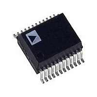
ADE7755ARS Analog Devices Inc, ADE7755ARS Datasheet - Page 3

ADE7755ARS
Manufacturer Part Number
ADE7755ARS
Description
IC ENERGY METERING 24-SSOP
Manufacturer
Analog Devices Inc
Datasheet
1.ADE7755ARSZRL.pdf
(20 pages)
Specifications of ADE7755ARS
Rohs Status
RoHS non-compliant
Input Impedance
390 KOhm
Measurement Error
0.1%
Voltage - I/o High
2.4V
Voltage - I/o Low
0.8V
Current - Supply
3mA
Voltage - Supply
4.75 V ~ 5.25 V
Operating Temperature
-40°C ~ 85°C
Mounting Type
Surface Mount
Package / Case
24-SSOP (0.200", 5.30mm Width)
Meter Type
Single Phase
For Use With
EVAL-ADE7755ZEB - BOARD EVALUATION FOR AD7755
Lead Free Status / RoHS Status
Not Compliant
Available stocks
Company
Part Number
Manufacturer
Quantity
Price
Part Number:
ADE7755ARS
Manufacturer:
ADI/亚德诺
Quantity:
20 000
Company:
Part Number:
ADE7755ARS/ADE7755
Manufacturer:
Panasonic
Quantity:
200
Part Number:
ADE7755ARSRL
Manufacturer:
ADI/亚德诺
Quantity:
20 000
Part Number:
ADE7755ARSZ
Manufacturer:
ADI/亚德诺
Quantity:
20 000
Company:
Part Number:
ADE7755ARSZ-RL
Manufacturer:
TI
Quantity:
230
Company:
Part Number:
ADE7755ARSZRL
Manufacturer:
FREESCALE
Quantity:
430
SPECIFICATIONS
AV
Table 1.
Parameter
ACCURACY
ANALOG INPUTS
REFERENCE INPUT
ON-CHIP REFERENCE
CLKIN
LOGIC INPUTS
LOGIC OUTPUTS
Measurement Error
Phase Error
AC Power Supply Rejection
DC Power Supply Rejection
Maximum Signal Levels
Input Impedance (DC)
−3 dB Bandwidth
ADC Offset Error
Gain Error
Gain Error Match
REF
Input Impedance
Input Capacitance
Reference Error
Temperature Coefficient
Input Clock Frequency
SCF, S0, S1, AC/DC, RESET, G0, and G1
F1 and F2
CF and REVP
DD
Gain = 1
Gain = 2
Gain = 8
Gain = 16
V1 Phase Lead 37° (PF = 0.8 Capacitive)
V1 Phase Lag 60° (PF = 0.5 Inductive)
Output Frequency Variation (CF)
Output Frequency Variation (CF)
Input High Voltage, V
Input Low Voltage, V
Input Current, I
Input Capacitance, C
Output High Voltage, V
Output Low Voltage, V
Output High Voltage, V
Output Low Voltage, V
= DV
IN/OUT
Input Voltage Range
1, 2
DD
1
1
3
= 5 V ± 5%, AGND = DGND = 0 V, on-chip reference, CLKIN = 3.58 MHz, T
Between Channels
3
1, 2
1
IN
1
on Channel 1
INL
IN
INH
OL
OL
OH
OH
1
1
Min
390
2.3
3.2
1
2.4
4.5
4
Typ
0.1
0.1
0.1
0.1
0.2
±0.3
14
±7
±0.2
±30
Rev. A | Page 3 of 20
Max
±0.1
±0.1
±1
±25
2.7
10
±200
4
0.8
±3
10
0.5
0.5
Unit
% reading
% reading
% reading
% reading
Degrees
Degrees
% reading
% reading
kΩ
kHz
mV
% ideal
V
V
kΩ
pF
mV
ppm/°C
MHz
V
V
μA
pF
V
V
V
V
V
% ideal
MHz
Test Conditions/Comments
Channel 2 with full-scale signal (±660 mV), 25°C
Over a dynamic range of 500 to 1
Over a dynamic range of 500 to 1
Over a dynamic range of 500 to 1
Over a dynamic range of 500 to 1
Line frequency = 45 Hz to 65 Hz
AC/DC = 0 and AC/DC = 1
AC/DC = 0 and AC/DC = 1
AC/DC = 1, S0 = S1 = 1, G0 = G1 = 0
V1 = 100 mV rms, V2 = 100 mV rms @ 50 Hz,
ripple on AV
AC/DC = 1, S0 = S1 = 1, G0 = G1 = 0
V1 = 100 mV rms, V2 = 100 mV rms,
AV
See the Analog Inputs section
CLKIN = 3.58 MHz
CLKIN/256, CLKIN = 3.58 MHz
Gain = 1
External 2.5 V reference, gain = 1
V1 = 470 mV dc, V2 = 660 mV dc
External 2.5 V reference
2.5 V + 8%
2.5 V − 8%
Nominal 2.5 V
Note all specifications for CLKIN of 3.58 MHz
DV
DV
Typically 10 nA, V
I
I
I
I
V1P, V1N, V2N, and V2P to AGND
SOURCE
SINK
SOURCE
SINK
DD
DD
DD
= 10 mA, DV
= 5 mA, DV
= DV
= 5 V ± 5%
= 5 V ± 5%
= 10 mA, DV
= 5 mA, DV
MIN
1, 2
DD
to T
DD
= 5 V ± 250 mV
MAX
of 200 mV rms @ 100 Hz
DD
DD
IN
DD
= 5 V
DD
= −40°C to +85°C.
= 5 V
= 0 V to DV
= 5 V
= 5 V
DD
ADE7755


