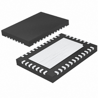
LTC4242IUHF#PBF Linear Technology, LTC4242IUHF#PBF Datasheet - Page 17

LTC4242IUHF#PBF
Manufacturer Part Number
LTC4242IUHF#PBF
Description
IC CTRLR HOTSWAP DUAL-SLOT 38QFN
Manufacturer
Linear Technology
Type
Hot-Swap Controllerr
Datasheet
1.LTC4242IUHFPBF.pdf
(24 pages)
Specifications of LTC4242IUHF#PBF
Applications
General Purpose, PCI Express
Internal Switch(s)
No
Voltage - Supply
2.7 V ~ 6 V
Operating Temperature
-40°C ~ 85°C
Mounting Type
Surface Mount
Package / Case
38-WFQFN, Exposed Pad
Lead Free Status / RoHS Status
Lead free / RoHS Compliant
Available stocks
Company
Part Number
Manufacturer
Quantity
Price
GATE Pin Voltage
The minimum gate drive voltage is 4.5V, therefore, logic
level N-channel MOSFETs should be used for the external
switches to maintain adequate gate enhancement. The
GATE pins are clamped at a typical value of 5.5V above
the respective OUT pins.
Compensating the Active Current Loop
The active current limit circuit is compensated using the
resistor R
of C
R
value range for R
APPLICATIO S I FOR ATIO
3V
G
3.3V
IN
value should be experimentally determined. A suggested
– 3V
ON/FAULT
G
3V
is selected based on the inrush current allowed. The
SENSE
3V
GATE
R
200k
13mΩ
IN
AUTO
G
R2
C
0.1µF
AUTO
and the slew rate control capacitor C
Figure 9. Auto-Retry Application
Figure 10. Auto-Retry Timing
3V
3V
FAULT
ON
G
SENSE
IN
Si7336ADP
is between 10Ω and 100Ω.
LTC4242*
U
3V
GND
Q2
1.235V
GATE
3V
*ADDITIONAL DETAILS OMITTED FOR CLARITY
U
OUT
EN
V
V
TH
CB
t
BD_PRST
CB
0.6V
V
OL
W
t
OFF
G
. The value
U
4242 F09
LOAD
4242 F10
V
The LTC4242 derives its power from V
of 1µF should be connected between this pin and ground.
If V
a lowpass fi lter shown in Figure 11 should be used.
This RC network allows the LTC4242 to ride through a
3V
below the V
narrow but high glitches due to parasitic inductance. Since
the absolute maximum rating for V
10V for AUXIN and 3V
chosen to damp the peak voltage seen by V
Force ON Operation
When the FON pin is pulled high and EN is low, the
LTC4242 operates in the diagnostic mode. All the input
supplies’ power switches are forced to turn on, regardless
of undervoltage conditions on the input supplies, status of
the ON pins and the fault latch. The contents in the fault
latch would be preserved during this time and no change
of state would occur after the part is confi gured to operate
in the diagnostic mode. If the output current exceeds the
ECB threshold, FAULT/AUXFAULT is pulled low immedi-
ately, but does not latch. The undervoltage lockout on V
turns off all the switches, regardless of the status of FON.
During thermal shutdown, the internal switch is shut off to
prevent overheating, even if FON is high. The main power
switches remain on as FON is high. Care must be taken to
ensure the outputs are not short circuited since there is
no current limit mechanism in diagnostic mode.
CC
IN
CC
Power Supply
/AUXIN short-circuit transient without collapsing
is derived from the input supplies of 3V
Figure 11. RC Network for V
CC
UVLO threshold. AUXIN or 3V
AUXIN
3V
OR
IN
IN
33
R
, the R
S
W
S
and C1 values should be
4242 F11
C1
1 F
CC
CC
CC
. A bypass capacitor
Filtering
is 7V compared to
V
LTC4242
CC
CC
IN
IN
below 7V.
or AUXIN,
may have
17
4242f
CC


