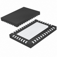
LTC4242IUHF#PBF Linear Technology, LTC4242IUHF#PBF Datasheet - Page 4

LTC4242IUHF#PBF
Manufacturer Part Number
LTC4242IUHF#PBF
Description
IC CTRLR HOTSWAP DUAL-SLOT 38QFN
Manufacturer
Linear Technology
Type
Hot-Swap Controllerr
Datasheet
1.LTC4242IUHFPBF.pdf
(24 pages)
Specifications of LTC4242IUHF#PBF
Applications
General Purpose, PCI Express
Internal Switch(s)
No
Voltage - Supply
2.7 V ~ 6 V
Operating Temperature
-40°C ~ 85°C
Mounting Type
Surface Mount
Package / Case
38-WFQFN, Exposed Pad
Lead Free Status / RoHS Status
Lead free / RoHS Compliant
Available stocks
Company
Part Number
Manufacturer
Quantity
Price
LTC4242
ELECTRICAL CHARACTERISTICS
temperature range, otherwise specifi cations are at T
(Note 2)
SYMBOL
V
ΔV
V
I
V
ΔV
I
V
I
I
R
Output Pins
V
I
Slew Rate
SR
Delays
t
t
t
t
Note 1: Stresses beyond those listed under Absolute Maximum Ratings
may cause permanent damage to the device. Exposure to any Absolute
Maximum Rating condition for extended periods may affect device
reliability and lifetime.
Note 2: All current into device pins is positive, all current out of the device
pins is negative. All voltages are referenced to GND unless otherwise
specifi ed.
4
ON(IN)
EN(UP)
SENSE
OUT
PU
PLH(GATE)
PLH(UVL)
PLH(PG)
PHL(SENSE)
ON(TH)
ON(RTH)
EN(TH)
FON
OL
OUT(DIS)
ON(TH)
EN(HYST)
AUXOUT
PARAMETER
ONn, AUXONn Pin Threshold Voltage
ONn, AUXONn Pin Hysteresis
ONn, AUXONn Pin Reset Threshold Voltage
ONn, AUXONn Pin Input Current
ENn Pin Threshold Voltage
ENn Pin Hysteresis
ENn Pull-Up Current
FONn Pin Logic Threshold
SENSE Pin Input Current
OUT Pin Input Current
OUT Pin Discharge Resistance
Output Low Voltage
Pull-Up Current
AUXOUTn Slew Rate
Input High (ONn) to GATEs High Prop Delay
Input Supply Low (12V
Low Prop Delay
Out Low (12V
Prop Delay
Sense Voltage High to GATE Low
12V
3V
12V
3V
12V
3V
AUXOUTn
FAULTn, AUXFAULTn, PGOODn,
AUXPGOODn (Note 5)
FAULTn, AUXFAULTn, PGOODn,
AUXPGOODn (Note 5)
SENSEn
OUTn
OUTn
SENSEn
OUTn
OUTn
OUTn
, 3V
OUTn
INn
, 3V
) to PGOOD High
INn
) to GATEs
A
= 25°C. V
CONDITIONS
Rising Edge
Falling Edge
V
ENn Rising
V
V
V
Gate Drive On
Gate Drive Off
I
V
ΔV
PIN
ONn
ENn
12VSENSEn
3VSENSEn
PIN
V
V
V
V
V
SENSE
AUXOUTn
12VOUTn
3VOUTn
12VOUTn
3VOUTn
The
= 3mA
= 1.5V
= 1V
= V
●
CC
AUXONn
= 200mV, C
= 3.3V
= 3.3V
= 2V
denotes the specifi cations which apply over the full operating
= 12V
= 6V
= 12V
= V
= 2V
AUXINn
Note 3: An internal clamp limits the GATE pins to a minimum of 5V above
V
device.
Note 4: For the QFN package, the AUX FET on resistance is guaranteed by
correlation to wafer level measurements.
Note 5: Available on QFN package only.
= 1.2V
OUT
. Driving this pin to voltages beyond the clamp may damage the
GATE
= V
= 10nF
3VINn
= 3.3V, V
12VINn
●
●
●
●
●
●
●
●
●
●
●
●
●
●
●
●
●
●
●
●
●
●
= 12V, unless otherwise noted.
1.173
1.173
MIN
350
165
375
0.5
0.7
30
30
–5
–5
1.235
1.235
0.14
1.25
TYP
700
330
750
0.6
0.4
70
70
–9
40
40
45
27
–9
18
20
7
1.297
1.297
1400
1500
MAX
120
120
–13
100
100
660
–13
0.7
2.6
0.4
1.7
±1
90
60
14
36
40
1
UNITS
V/ms
4242f
mV
mV
µA
µA
µA
µA
µA
µA
µA
µs
µs
µs
µs
Ω
Ω
Ω
V
V
V
V
V


