LM5067MW-1/NOPB National Semiconductor, LM5067MW-1/NOPB Datasheet - Page 5
LM5067MW-1/NOPB
Manufacturer Part Number
LM5067MW-1/NOPB
Description
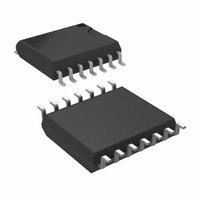
IC CTLR NEG HOTSWAP LATCH 14SOIC
Manufacturer
National Semiconductor
Type
Hot-Swap Controllerr
Datasheet
1.LM5067MM-1NOPB.pdf
(24 pages)
Specifications of LM5067MW-1/NOPB
Applications
General Purpose
Internal Switch(s)
No
Voltage - Supply
-9 V ~ -80 V
Operating Temperature
-40°C ~ 125°C
Mounting Type
Surface Mount
Package / Case
14-SOIC (0.300", 7.50mm Width)
Linear Misc Type
Negative Voltage
Family Name
LM5067-1
Operating Supply Voltage (min)
-9V
Operating Supply Voltage (max)
-80V
Operating Temperature (min)
-40C
Operating Temperature (max)
125C
Operating Temperature Classification
Automotive
Product Height (mm)
2.35mm
Mounting
Surface Mount
Pin Count
14
Lead Free Status / RoHS Status
Lead free / RoHS Compliant
Other names
LM5067MW-1
Available stocks
Company
Part Number
Manufacturer
Quantity
Price
Company:

Part Number:
LM5067MW-1/NOPB
Manufacturer:
TI/NS
Quantity:
2 600


Current Limit
Circuit Breaker
Power Limit (PWR Pin)
Timer (TIMER Pin)
Power Good (PGD Pin)
Thermal Resistance (Note 6)
Note 1: Absolute Maximum Ratings indicate limits beyond which damage to the device may occur. Operating Ratings indicate conditions for which the device is
intended to be functional, but do not guarantee specific performance limits. For guaranteed specifications and conditions see the Electrical Characteristics.
Note 2: The human body model is a 100 pF capacitor discharged through a 1.5 kΩ resistor into each pin.
Note 3: Current out of a pin is indicated as a negative value.
Note 4: For detailed information on soldering plastic MSOP package refer to the Packaging Databook available from National Semiconductor Corporation.
Note 5: Maximum continuous current into VCC is limited by power dissipation and die temperature. See the Thermal Considerations section.
Note 6: Tested on a 4 layer JEDEC board with 2 vias under the package. See JEDEC standards JESD51-7 and JESD51-3. See the Thermal Considerations
section.
Note 7: N/C Pins are internally not connected to anything.
DC
Symbol
PWR
PGD
PGD
PGD
V
V
t
I
FAULT
I
TIMER
V
V
θ
θ
PWR
TMRH
θ
θ
t
t
TMRL
FAULT
CL
CB
CB
CL
JA
JC
JA
JC
VOL
IOH
LIM
TH
Parameter
Threshold voltage
Response time
Threshold voltage
Response time
Power limit sense voltage (SENSE - VEE)
PWR pin current
Upper threshold
Lower threshold
Insertion time current
Sink current, end of insertion time
Fault detection current
Sink current, end of fault time
Fault Restart Duty Cycle
Fault to GATE low delay
Threshold measured at OUT - SENSE
Output low voltage
Off leakage current
Junction to Ambient
Junction to Case
Junction to Ambient
Junction to Case
5
Conditions
SENSE - VEE voltage
SENSE - VEE stepped from 0 mV
to 80 mV
SENSE - VEE voltage
SENSE - VEE stepped from 0 mV
to 150 mV, time to GATE low, no
load
OUT - SENSE = 24V, R
kΩ
V
Restart cycles (LM5067-2)
End of 8th cycle (LM5067-2)
Re-enable threshold (LM5067-1)
TIMER pin = 2V
TIMER pin = 2V
TIMER pin = 2V
LM5067-2
TIMER pin reaches 4.0V
Decreasing
Increasing, relative to decreasing
threshold
I
V
MSOP package
MSOP package
SO-14 Package
SO-14 Package
SINK
PWR
PGD
= 2 mA
= 80V
= 2.5V
PWR
= 75
1.162 1.23 1.285
1.143 1.25 1.325
-140
16.5
3.76
1.18
Min
-9.5
1.2
0.9
44
70
0.65
1.25
1.55
Typ
100
-23
-85
0.3
0.3
2.5
0.5
50
25
22
15
60
94
44
90
27
-6
4
www.national.com
Max
27.5
4.16
1.32
4.25
130
-2.5
150
1.0
1.9
-44
56
5
Units
°C/W
°C/W
°C/W
°C/W
mV
mV
mV
mA
mV
µA
µA
µA
µA
µA
µs
µs
µs
%
V
V
V
V
V
Related parts for LM5067MW-1/NOPB
Image
Part Number
Description
Manufacturer
Datasheet
Request
R

Part Number:
Description:
National Semiconductor [8-Bit D/A Converter]
Manufacturer:
National Semiconductor
Datasheet:
Part Number:
Description:
National Semiconductor [Media Coprocessor]
Manufacturer:
National Semiconductor
Datasheet:
Part Number:
Description:
Digitally Controlled Tone and Volume Circuit with Stereo Audio Power Amplifier, Microphone Preamp Stage and National 3D Sound
Manufacturer:
National Semiconductor
Datasheet:
Part Number:
Description:
Digitally Controlled Tone and Volume Circuit with Stereo Audio Power Amplifier, Microphone Preamp Stage and National 3D Sound
Manufacturer:
National Semiconductor
Datasheet:
Part Number:
Description:
AC97 Rev 2 Codec with Sample Rate Conversion and National 3D Sound
Manufacturer:
National Semiconductor
Part Number:
Description:
Manufacturer:
National Semiconductor
Datasheet:
Part Number:
Description:
Manufacturer:
National Semiconductor
Datasheet:
Part Number:
Description:
General Purpose, Low Voltage, Low Power, Rail-to-Rail Output Operational Amplifiers
Manufacturer:
National Semiconductor
Datasheet:
Part Number:
Description:
8-bit 20 MSPS flash A/D converter.
Manufacturer:
National Semiconductor
Datasheet:
Part Number:
Description:
Low Noise Quad Operational Amplifier
Manufacturer:
National Semiconductor
Datasheet:
Part Number:
Description:
Quad Differential Line Receivers
Manufacturer:
National Semiconductor
Datasheet:
Part Number:
Description:
Quad High Speed Trapezoidal? Bus Transceiver
Manufacturer:
National Semiconductor
Datasheet:
Part Number:
Description:
Dual Line Receiver
Manufacturer:
National Semiconductor
Datasheet:
Part Number:
Description:
TTL to 10k ECL Level Translator with Latch
Manufacturer:
National Semiconductor
Datasheet: