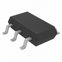
LTC4210-1IS6#TRPBF Linear Technology, LTC4210-1IS6#TRPBF Datasheet - Page 15

LTC4210-1IS6#TRPBF
Manufacturer Part Number
LTC4210-1IS6#TRPBF
Description
IC CONTROLLER HOT SWAP TSOT23-6
Manufacturer
Linear Technology
Type
Hot-Swap Controllerr
Datasheet
1.LTC4210-1CS6TRMPBF.pdf
(20 pages)
Specifications of LTC4210-1IS6#TRPBF
Applications
General Purpose
Internal Switch(s)
No
Voltage - Supply
2.7 V ~ 16.5 V
Operating Temperature
-40°C ~ 85°C
Mounting Type
Surface Mount
Package / Case
SOT-23-6 Thin, TSOT-23-6
Linear Misc Type
Positive Low Voltage
Family Name
LTC4210-1
Package Type
TSOT-23
Operating Supply Voltage (min)
2.7V
Operating Supply Voltage (max)
16.5V
Operating Temperature (min)
-40C
Operating Temperature (max)
85C
Operating Temperature Classification
Industrial
Product Height (mm)
0.9mm
Product Length (mm)
2.9mm
Mounting
Surface Mount
Pin Count
6
Lead Free Status / RoHS Status
Lead free / RoHS Compliant
Available stocks
Company
Part Number
Manufacturer
Quantity
Price
Part Number:
LTC4210-1IS6#TRPBFLTC4210-1IS6#TRMPBF
Manufacturer:
LINEAR/凌特
Quantity:
20 000
APPLICATIO S I FOR ATIO
Table 1. t
Normal Mode/External Timer Control
Whenever the TIMER pin voltage drops below the COMP1
threshold, but is not in reset mode, the TIMER enters
normal (100 A source) mode with an equivalent 7k resis-
tive pull-down. Table 1 shows the relationship of t
t
If the TIMER pin is pulled beyond the COMP2 threshold,
the GATE pin is pulled to ground immediately. This allows
the TIMER pin to be used for overvoltage detection, see
Figure 11.
Externally forcing the TIMER pin below the COMP1 thresh-
old will reset the TIMER to normal mode. During overvolt-
age detection, the TIMER’s 100 A pull-down current will
continue to be on if (V
If the (V
overvoltage detection, the TIMER current will be the same
as described for latched-off or autoretry mode. See the
CBDELAY
C
TIMER
0.033
0.047
0.068
0.082
0.22
0.33
0.47
0.68
0.82
0.1
2.2
3.3
1
INITIAL
( F)
CC
, t
COOLOFF
– SENSE) voltage exceeds 50mV during the
, t
CBDELAY
t
INITIAL
128.3
185.6
223.8
272.9
600.5
900.7
12.8
18.6
22.4
27.3
60.0
90.1
9.0
vs C
U
(ms)
CC
, t
TIMER
COOLOFF
– SENSE) voltage is below 50mV.
U
t
.
CBDELAY
vs C
10.2
14.7
17.8
21.7
47.7
71.5
0.7
1.5
1.8
2.2
4.8
7.2
1
TIMER
W
(ms)
t
COOLOFF
181.5
258.5
U
1210
1815
18.2
25.9
37.4
45.1
121
374
451
550
55
INITIAL
(ms)
,
section OVERVOLTAGE DETECTION USING TIMER PIN
for details of the application.
Power-Off Cycle
The system can be reset by toggling the ON pin low for
more than 30 s as shown at time point 7 of Figure 3. The
GATE pin is pulled to ground. The TIMER capacitor is also
discharged to ground. C
Alternatively, the TIMER pin can be externally driven above
the COMP2 threshold to turn off the GATE pin.
POWER MOSFET SELECTION
Power MOSFETs can be classified by R
drive ratings of 10V, 4.5V, 2.5V and 1.8V. Use the typical
curves VGATE vs Supply Voltage and VGATE vs Tem-
perature to determine whether the gate drive voltage is
adequate for the selected MOSFET at the operating volt-
age.
In addition, the selected MOSFET should fulfill two V
criteria:
1. Positive V
2. Negative V
If one of the conditions cannot be met, an external Zener
clamp shown on Figure 10a or Figure 10b can be used. The
selection of R
package dissipation when discharging V
clamp.
maximum V
voltage. The gate of the MOSFET can discharge faster
than V
C
LOAD
.
OUT
GS
when shutting down the MOSFET with a large
GS
G
absolute maximum rating > LTC4210
GATE
LTC4210-1/LTC4210-2
should be within the allowed LTC4210
absolute maximum rating > supply
, and
LOAD
discharges through the load.
DSON
OUT
via the Zener
at V
15
GS
421012f
gate
GS


