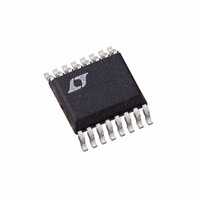
LT4256-3CGN Linear Technology, LT4256-3CGN Datasheet - Page 7

LT4256-3CGN
Manufacturer Part Number
LT4256-3CGN
Description
IC CTRLR HOTSWP HV DETECT 16SSOP
Manufacturer
Linear Technology
Type
Hot-Swap Controllerr
Datasheet
1.LT4256-3IGNPBF.pdf
(20 pages)
Specifications of LT4256-3CGN
Applications
General Purpose
Internal Switch(s)
No
Voltage - Supply
10.8 V ~ 80 V
Operating Temperature
0°C ~ 70°C
Mounting Type
Surface Mount
Package / Case
16-SSOP (0.150", 3.90mm Width)
Family Name
LT4256-3
Package Type
SSOP N
Operating Supply Voltage (min)
10.8V
Operating Supply Voltage (max)
80V
Operating Temperature (min)
0C
Operating Temperature (max)
70C
Operating Temperature Classification
Commercial
Product Depth (mm)
3.99mm
Product Height (mm)
1.5mm
Mounting
Surface Mount
Pin Count
16
Lead Free Status / RoHS Status
Contains lead / RoHS non-compliant
Lead Free Status / RoHS Status
Contains lead / RoHS non-compliant
Available stocks
Company
Part Number
Manufacturer
Quantity
Price
Company:
Part Number:
LT4256-3CGN
Manufacturer:
LT
Quantity:
10 000
Part Number:
LT4256-3CGN
Manufacturer:
LT/凌特
Quantity:
20 000
Part Number:
LT4256-3CGN#PBF
Manufacturer:
LINEAR/凌特
Quantity:
20 000
Part Number:
LT4256-3CGN#TRPBF
Manufacturer:
LINEAR/凌特
Quantity:
20 000
PI FU CTIO S
GATE (Pin 13): High Side Gate Drive for the External
N-Channel MOSFET. An internal charge pump guarantees
at least 10V of gate drive for V
20V and 4.5V of gate drive for V
between 10.8V and 20V. The rising slope of the voltage on
GATE is set by an external capacitor connected from GATE
to GND and an internal 32µA pull-up current source from
the charge pump output.
If the current limit is reached, the GATE voltage is adjusted
to maintain a constant voltage across the sense resistor
while the timing capacitor starts to charge. If the TIMER
voltage ever exceeds 4.65V, GATE is pulled low.
GATE is also pulled to GND whenever UV is pulled low; the
V
undervoltage threshold, above the overvoltage threshold
or below the internal UVLO threshold (9.8V).
GATE is clamped internally to a maximum voltage of
11.6V (typ) above V
tions. Driving this pin beyond the clamp voltage may
damage the part. GATE is also clamped to 2V (typ) below
V
condition, it is discharged quickly by a 62mA (typ)
CC
OUT
U
supply voltage drops below the externally programmed
. When the gate is commanded off due to a fault
U
OUT
U
under normal operating condi-
CC
supply voltages above
CC
supply voltages
capable switch until GATE is 2V (typ) below V
GATE is below V
to protect the LT4256-3 against damage if V
capacitance. A Zener diode is needed between the gate
and source of the external MOSFET to protect its gate
oxide under instantaneous short-circuit conditions. See
Applications Information.
SENSE (Pin 15): Current Limit Sense Input. A sense
resistor is placed in the supply path between V
SENSE. The current limit circuit regulates the voltage
across the sense resistor (V
current limit when FB is 2V or higher. If FB drops below
2V, the regulated voltage across the sense resistor de-
creases linearly and stops at 14mV when FB is 0V. The
OPEN output also uses SENSE to detect when the output
current is less than (3mV)/R5.
To defeat current limit, connect SENSE to V
V
input ranges from 10.8V to 80V for normal operation. I
is typically 1.8mA. An internal circuit disables the LT4256-3
for inputs less than 9.8V (typ).
CC
(Pin 16): Input Supply Voltage. The positive supply
OUT
by 2V, the 62mA is reduced to 130µA
CC
– SENSE) to 55mV while in
LT4256-3
OUT
CC
OUT
.
has large
. When
CC
42563fa
and
7
CC


