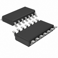
LTC1645CS#TR Linear Technology, LTC1645CS#TR Datasheet - Page 12

LTC1645CS#TR
Manufacturer Part Number
LTC1645CS#TR
Description
IC CTRLR SEQ HOTSWAP DUAL 14SOIC
Manufacturer
Linear Technology
Type
Hot-Swap Controllerr
Datasheet
1.LTC1645CS8PBF.pdf
(24 pages)
Specifications of LTC1645CS#TR
Applications
General Purpose
Internal Switch(s)
No
Voltage - Supply
1.2 V ~ 12 V
Operating Temperature
0°C ~ 70°C
Mounting Type
Surface Mount
Package / Case
14-SOIC (0.154", 3.90mm Width)
Lead Free Status / RoHS Status
Contains lead / RoHS non-compliant
Available stocks
Company
Part Number
Manufacturer
Quantity
Price
APPLICATIO S I FOR ATIO
LTC1645
nearly unlimited current flow. The LTC1645 discharges
the GATE pin in a few microseconds, but during this
discharge time current on the order of 150 amperes flows
from the V
power supply, causing V
On recovery from overload, some supplies may over-
shoot. Other devices attached to this supply may reset or
malfunction and the overshoot may also damage some
components. An inductor (1 H to 10 H) in series with the
FET’s source limits the short-circuit di/dt, thereby limiting
the peak current and the supply glitch (Figure 8c and 8d).
Additional power supply bypass capacitance also reduces
the magnitude of the V
Reset
The LTC1645 uses an internal 1.238V bandgap reference,
a precision voltage comparator, and a resistive divider to
monitor the output supply voltage (Figure 9).
Whenever the voltage at the FB pin rises above its reset
threshold (1.238V), the comparator output goes high, and
a timing cycle starts (see Figure 10, time points 1 and 4).
After a complete timing cycle, RESET is released. An
external pull-up is required for the RESET pin to rise to a
logic high.
When the voltage at the FB pin drops below its reset
threshold, the comparator output goes low. After passing
through a glitch filter, RESET is pulled low (time point 2).
If the FB pin rises above the reset threshold for less than
a timing cycle, the RESET output remains low (time
point 3).
12
ON
CC
TIMER
LOGIC
Figure 9. Supply Monitor Block Diagram
power supply. This current spike glitches the
TIMER
C
TIMER
U
REFERENCE
1.238V
COMP
CC
CC
U
glitch.
to dip (Figure 8a and 8b).
+
–
W
RESET
FB
U
10k
V
OUT
1645 F09
RESET
P
Glitch Filter
The LTC1645 has a glitch filter to prevent RESET from
generating a spurious system reset in the presence of
transients on the FB pin. The filter is 20 s for large
transients (greater than 150mV) and up to 80 s for
smaller transients. The relationship between glitch filter
time and the transient voltage is shown in Typical Perfor-
mance Characteristics: Glitch Filter Time vs Feedback
Transient.
Timer
The system timing for the LTC1645 is generated by the
circuitry shown in Figure 11. The timer is used to set the
turn-on delay after the ON pin goes high. It also sets the
delay before the RESET pin goes high after the FB pin
exceeds 1.238V.
Whenever the timer is off, the internal N-channel shorts
the TIMER pin to ground (Figure 11). Activating the timer
connects a 2 A current from V
ON
TIMER
RESET
V
OUT
Figure 11. System Timing Block Diagram
Figure 10. Supply Monitor Waveforms
V2
TIMER
2 A
1.23V
C
1
TIMER
1.23V
+
–
2
V1
COMP
V2
CC1
3
to the TIMER pin and the
LOGIC
V1 V2
4
MONITOR
1.23V
SUPPLY
1645 F10
1645 F11
1645fa


