LTC1645CS#TR Linear Technology, LTC1645CS#TR Datasheet - Page 14

LTC1645CS#TR
Manufacturer Part Number
LTC1645CS#TR
Description
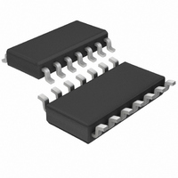
IC CTRLR SEQ HOTSWAP DUAL 14SOIC
Manufacturer
Linear Technology
Type
Hot-Swap Controllerr
Datasheet
1.LTC1645CS8PBF.pdf
(24 pages)
Specifications of LTC1645CS#TR
Applications
General Purpose
Internal Switch(s)
No
Voltage - Supply
1.2 V ~ 12 V
Operating Temperature
0°C ~ 70°C
Mounting Type
Surface Mount
Package / Case
14-SOIC (0.154", 3.90mm Width)
Lead Free Status / RoHS Status
Contains lead / RoHS non-compliant
Available stocks
Company
Part Number
Manufacturer
Quantity
Price
APPLICATIO S I FOR ATIO
LTC1645
An external hard reset is initiated at time point 6. The ON
pin is forced below 0.8V but above 0.4V, and the GATE n
pin voltages start to ramp down. V
down, and RESET goes low when V
power-good trip level at time point 7.
Time points 8 to 15 are similar to time points 1 to 7, except
the ON pin’s different voltage thresholds are used to ramp
V
goes above 0.8V but below 2V, and one timing cycle later
(time point 9) GATE1 begins to ramp up with V
following one gate-to-source voltage drop lower. At time
point 10, the ON pin goes above 2V and GATE2 immedi-
ately begins ramping up with V
source voltage drop lower. As soon as V
power-good trip level at time point 11, a timing cycle
starts. At the end of the timing cycle (time point 12),
RESET goes high and the power-up process is complete.
The ON pin is forced below 2V but above 0.8V at time point
13 and the GATE2 pin voltage starts to ramp down. V
also starts to ramp down and RESET goes low when V
drops below the power-good trip level at time point 14.
When the ON pin goes below 0.8V but above 0.4V at time
point 15, GATE1 and V
14
OUT1
and V
3.3V
2.5V
V
V
IN1
IN2
OUT2
BOTH CURRENT LIMITS: 5A
POINT:
1.37k
1%
1.18k
1%
separately. At time point 8, the ON pin
TRIP
U
3V
OUT1
4.99k
1%
1.82k
1%
*WSL1206-01-1% (VISHAY DALE)
U
ramp down.
OUT2
10
10k
4
OUT n
Figure 15. Ramping 3.3V and 2.5V Up and Down Together
ON
FAULT
W
following one gate-to-
OUT2
V
CC1
0.01 *
also starts to ramp
14
TIMER
SENSE1
drops below the
OUT2
13
11
0.33 F
reaches its
U
GATE1
(14-LEAD)
LTC1645
12
OUT1
OUT2
OUT2
V
CC2
0.01 *
1
SENSE2
GND
2
7
1/2 Si4920DY
COMPOUT
Time points 16 to 19 show the same power-up sequence
as time points 2 to 5, while time point 20 demonstrates the
GATE n pins being pulled immediately to ground (instead
of ramping down) by the ON pin going below 0.4V.
Power Supply Tracking and Sequencing Applications
The LTC1645 is able to sequence V
ways, including ramping V
ramping V
first and V
V
Figure 15 shows an application ramping V
up and down together. The ON pin must reach 0.8V to
ramp up V
ON pin low until V
reach 0.8V before V
supplies must be within regulation before a timing cycle
can start. At the end of the timing cycle, the output voltages
ramp up together. If either input supply falls out of
regulation, the gates of Q1 and Q2 are pulled low together.
Figure 16 shows an oscilloscope photo of the circuit in
Figure 15.
OUT1
GATE2
COMP
RESET
Q2
3
10
FB
1/2 Si4920DY
+
and V
8
9
6
5
Q1
OUT1
OUT1
10
OUT1
0.1 F
25V
OUT2
1645 F15
and V
up first and down first; ramping V
and V
CC2
up and down together.
D1
1N4002
D2
1N4002
1.18k
1%
1.37k
1%
OUT2
is above 2.3V, and the ON pin cannot
CC1
OUT2
. The spare comparator pulls the
is above 3V. Thus, both input
D3
MBR0530T1
10k
OUT1
down together; and ramping
up first and down last;
+
+
OUT n
C
C
LOAD1
LOAD2
P RESET
OUT1
in a number of
V
3.3V
2.5A
V
2.5V
2.5A
OUT1
OUT2
and V
OUT1
OUT2
1645fa
up


