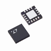
LTC5100EUF#TR Linear Technology, LTC5100EUF#TR Datasheet - Page 21

LTC5100EUF#TR
Manufacturer Part Number
LTC5100EUF#TR
Description
IC DRIVER VCSEL 3.2GBPS 16QFN
Manufacturer
Linear Technology
Type
Laser Diode Driverr
Datasheet
1.LTC5100EUF.pdf
(52 pages)
Specifications of LTC5100EUF#TR
Data Rate
3.2Gbps
Number Of Channels
1
Voltage - Supply
3.135 V ~ 3.465 V
Current - Supply
54mA
Current - Modulation
12mA
Operating Temperature
-40°C ~ 85°C
Package / Case
16-QFN
Mounting Type
Surface Mount
Lead Free Status / RoHS Status
Contains lead / RoHS non-compliant
Lead Free Status / RoHS Status
Contains lead / RoHS non-compliant
Available stocks
Company
Part Number
Manufacturer
Quantity
Price
OPERATIO
Figure 19 shows how the LTC5100 achieves a low reflec-
tion coefficient. The unavoidable capacitance of the high
speed driver transistor, bond pads and ESD protection
circuitry (C1) is compensated by the inductance of the
bond wires (L
The high speed behavior of the circuit in Figure 19 can be
understood in greater detail by examining the simplified
circuit in Figure 20. In Figure 20 the switched current
source (M1 in Figure 19) launches a current step (1)
toward the termination resistor (2A) and toward the trans-
mission line (2B) connected to the laser. The laser is
typically mismatched to the line impedance and reflects a
portion of the incident wave (3) back toward the MODB
pin. There it encounters an L-C-L structure composed of
the bond wires and driver capacitance. This structure is
carefully designed as a lumped element approximation to
the transmission line impedance. It therefore transmits
wave (3) through the IC package without reflecting energy
back toward the laser. The traveling wave passes through
the chip largely unimpeded (4) and is absorbed by the
matched termination resistor, R
The matched termination is provided by the termination
resistor, R
short across the entire frequency range contained in the
modulation data.
The termination resistor, R
for electrical testing because it matches the impedance of
most high frequency instruments. R
35 , for example, to more closely match a laser with low
dynamic impedance or to allow more voltage headroom at
the SRC pin. This may be necessary for lasers that run at
high voltages or high bias currents. R
70 for example, to more closely match a laser with high
Figure 20. Wave Propagation in the Laser Interconnect
R
50
TYP
T
2A
MODA
11
4
T
, decoupled by capacitor C
L
BWA
BWA
U
and L
C1
BWB
T
, need not be 50 . 50 is best
L
1
).
BWB
T
MODB TRANSMISSION
.
10
T
2B
can be made smaller,
T
can be made larger,
T
. C
Z
LINE
O
T
= R
forms an AC
T
3
5100 F20
dynamic impedance or if a narrow, high impedance PC
board trace is needed to connect to the laser.
Figure 21 shows that the high speed modulation current is
confined to the ground system, laser and back termination
network. No high speed current circulates in the power
supply where it could cause radiation and interference
problems.
HIGH SPEED DATA INPUTS
The high speed data inputs, IN
terminated in 50 and internally AC coupled, eliminating
the need for external termination resistors and AC cou-
pling capacitors. Figure 10 shows the equivalent circuit
for the high speed data pins. By default, the high speed
data inputs are terminated differentially with 100
compatibility with LVDS, PECL and similar differential
signaling standards (Cml_en = 0). Alternately, the inputs
can be programmed for 50 single-ended termination to
the power supply for biasing a current mode logic (CML)
driver. To select CML compatibility, program Cml_en to 1.
Although internally AC coupled, the inputs are biased with
high valued resistors (50k equivalent) to V
LTC5100 remains compatible with external AC coupling
capacitors. When externally AC coupled, the inputs self-
bias to approximately V
Internal AC coupling gives the LTC5100 rail-to-rail input
common mode capability. The inputs can be driven as
much as 300mV beyond the rail during peak excursions.
The AC coupling circuit is a distributed highpass filter with
Figure 21. High Speed Current Flow in the Modulation Output
LTC5100
MODULATOR
3.2Gbps
V
DD(HS)
DD
M1
V
SS
/2.
EXPOSED
PAD
MODA
MODB
+
SRC
and IN
14
11
12
10
9
5100 F21
LTC5100
CURRENT
NO HIGH
–
DD(HS)
SPEED
, are internally
50
/2, so the
sn5100 5100fs
10nF
21
for


