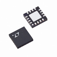
LTC5100EUF#TR Linear Technology, LTC5100EUF#TR Datasheet - Page 3

LTC5100EUF#TR
Manufacturer Part Number
LTC5100EUF#TR
Description
IC DRIVER VCSEL 3.2GBPS 16QFN
Manufacturer
Linear Technology
Type
Laser Diode Driverr
Datasheet
1.LTC5100EUF.pdf
(52 pages)
Specifications of LTC5100EUF#TR
Data Rate
3.2Gbps
Number Of Channels
1
Voltage - Supply
3.135 V ~ 3.465 V
Current - Supply
54mA
Current - Modulation
12mA
Operating Temperature
-40°C ~ 85°C
Package / Case
16-QFN
Mounting Type
Surface Mount
Lead Free Status / RoHS Status
Contains lead / RoHS non-compliant
Lead Free Status / RoHS Status
Contains lead / RoHS non-compliant
Available stocks
Company
Part Number
Manufacturer
Quantity
Price
temperature range, otherwise specifications are at T
resistor from SRC (Pin 14) to MODA (Pin 11); 50 , 1% load AC coupled to MODB (Pin 10); 10nF, 10% capacitor from SRC (Pin 14) to
V
PARAMETER
Laser Bias Current, I
Full-Scale Current (Note 8)
Absolute Accuracy
Resolution
Linear Tempco Resolution
Linear Tempco Range
Second Order Tempco Resolution
Second Order Tempco Range
Temperature Stability
Off-State Leakage
MODA, MODB Pin Current, I
Full Scale, Peak-to-Peak Modulation Current (Note 9)
Minimum Operating Current (Note 10)
Resolution (Note 11)
Current Stability
Voltage Range
Absolute Accuracy of the Modulation Current
Linear Tempco Resolution
Linear Tempco Range
Second Order Tempco Resolution
Second Order Tempco Range
Maximum Bit Rate
Modulation Current Rise and Fall Times
Deterministic Jitter, Peak-to-Peak (Note 12)
Random Jitter, RMS (Note 13)
Pulse Width Distortion
Automatic Power Control (Note 14)
Minimum Operating Current for the Monitor Diode
(Note 15)
Temperature Stability
Monitor Diode Bias Voltage (Note 16)
ELECTRICAL CHARACTERISTICS
SS
; Cml_en = 0, Lpc_en = 1, transmitter enabled, unless otherwise noted. Test circuit in Figure 5.
B
M
CONDITIONS
Is_rng = 0
Is_rng = 1
Is_rng = 2
Is_rng = 3
SRC Pin and MODA, MODB Pin Currents Within
Specified Voltage Ranges
Ib_tc1 = 0, Ib_tc2 = 0
Transmitter Disabled, V
Im_rng = 0
Im_rng = 1
Im_rng = 2
Im_rng = 3
Im_tc1 = 0, Im_tc2 = 0
Peak Transient Voltage on MODA and MODB
20% to 80% Measured with K28.5 Pattern at
2.5Gbps
Measured with K28.5 Pattern at 3.2Gbps
Imd_tc1 = 0, Imd_tc2 = 0
I
MD
A
= 25 C; V
1600 A
The
DD
denotes the specifications which apply over the full operating
= V
DD(HS)
SRC
= 1.2V
= 3.3V, I
S
= 24mA; I
M
= 12mA (I
1/8 of Full-Scale Peak-to-Peak
12 – I
18 – I
24 – I
6 – I
MIN
1.2
12
18
24
6
Monitor Diode Current
Modulation Current
M
20% of Full Scale
M
M
M
MPP
18 – I
27 – I
36 – I
9 – I
15625
15625
3.81
3.81
1.45
TYP
122
122
3.2
60
10
10
488
500
18
27
36
500
484
10
500
= 24mA); 49.9 , 1%
25
9
9
25
1
M
LTC5100
M
M
M
MAX
2.7
50
sn5100 5100fs
ppm/ C
ppm/ C
ppm/ C
ppm/ C
ppm/ C
ppm/ C
ppm/ C
ppm/ C
ppm/ C
ppm/ C
ppm/ C
UNITS
ps
Gbps
3
RMS
Bits
Bits
mA
mA
mA
mA
mA
mA
mA
mA
ps
ps
ps
%
%
A
V
V
2
2
2
2


